3
\$\begingroup\$

I am currently using a TLE2144, and the input signal of 600 kHz, 4.5 Vpp is generated from a function generator.

Using a voltage follower with TLE2144, I was able to get an output of 4.5 Vpp with an input from the function generator, but after it reaches above 510 kHz, the signal starts to distort on the negative cycle.

The gain bandwidth of TLE2144 is around 5 MHz, and the slew rate is 27 V/μs. Therefore, I should be getting a good signal on the output, yet the negative cycle of the signal looks slightly distorted. Not sure what the issue is. I do not know what I need to look for.

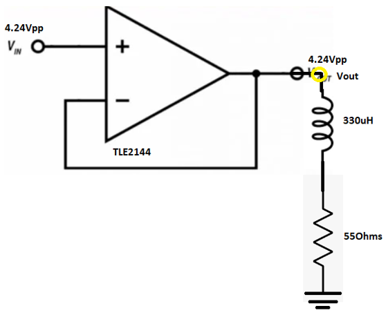
Schematic:

Dual Supply of +/-12 V enter image description here

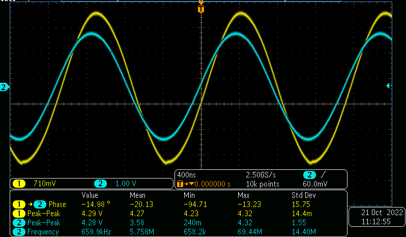
Image shown below (input: cyan signal, output: yellow signal):

I don't care about the phase difference.

enter image description here

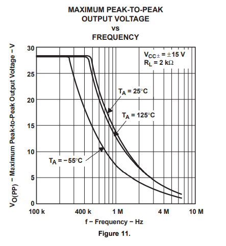
I may have found the issue; even though it mentions that for rhe TLE2144IDW, the gain-bandwidth is 5.9 Mhz, they have provided a chart where the signal starts attenuating after 500 kHz. I will have to look into this more.

enter image description here

\$\endgroup\$
8
  • 2
    \$\begingroup\$ Your open-loop gain is less than 10 typically @ 600kHz so you can't expect to see all that perfect an output. \$\endgroup\$ Commented Oct 21, 2022 at 19:44
  • \$\begingroup\$ @SpehroPefhany, how were you able to calculate that, I am only able to see open-loop output impedance of 30Ohms at 1MHz on datasheet. \$\endgroup\$ Commented Oct 21, 2022 at 19:57
  • 2
    \$\begingroup\$ Not so complicated. G * BW = 5.8MHz according to the datasheet, so for 600kHz BW, G < 10. \$\endgroup\$ Commented Oct 21, 2022 at 20:29
  • \$\begingroup\$ @SpehroPefhany I am using a voltage follower which is a closed loop gain with unity gain (Gain of 1) Why are you mentioning about open loop gain? I have looked for the word "Open loop gain", and I cannot find any information from the datasheet. On page 48, Figure 12, Voltage peak to peak vs frequency, is this what you are talking about? \$\endgroup\$ Commented Oct 21, 2022 at 22:01
  • 2
    \$\begingroup\$ @SamShurp The closed loop gain is equal to Vout/Vin. The open loop gain is equal to Vout divided by the difference between the op amp's actual inputs. The open loop gain has a very high value at low frequency but falls at -6 dB/octave as frequency increases. The amount of distortion is dependant on the amount of negative feedback which is dependent on the open loop gain value and the feedback fraction (unity in your case). I'm not saying that what you are seeing is due to reducing open loop gain but distortion does increase with increasing frequency as open loop gain and feedback reduce. \$\endgroup\$
    – user173271
    Commented Oct 21, 2022 at 23:02

4 Answers 4

3
\$\begingroup\$

If the 330µH inductor has a high enough self-resonance frequency and does not begin to behave as a capacitor at 600kHz, then its impedance will be pretty high and with 4.2Vpp at the input it should limit output current to a very reasonable +/- 1.7mA. So it's not an output current problem.

The opamp is used at a relatively high frequency compared to its gain bandwidth product: it has 6MHz GBW, so at 600kHz, only an open loop gain of 10 (20dB) remains to correct nonlinearities. From the internal schematic, internal compensation doesn't seem to wrap around the output stage, so only global feedback can reduce distortion in the output stage. However, the amount of feedback that counts towards reducing a certain distortion harmonic does not depend on the open loop gain at the fundamental frequency, but at the frequency of the harmonic in question. So, for example, to correct harmonic 2 at 1.2MHz, it loses 6dB of feedback, leaving only 5 (14dB). And for harmonic 4, only 8dB of feedback remains.

As frequency increases, crossover distortion will increase too, and feedback available to correct it is reduced. If the output stage is not included in the compensation, this causes a sharp rise in THD at high frequency, as shown by the datasheet:
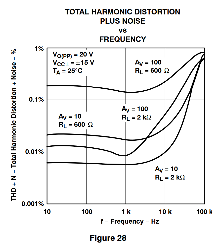
enter image description here

This is in agreement with your measurement: due to the inductor, current is shifted by almost 90°, so the output stage crossover will occur on the peaks of the output voltage waveform, right where a kink appears on your output voltage. The output stage is not symmetrical, and both sides will switch at different speeds, so it is not surprising the distortion is not symmetrical and only occurs on one polarity of the signal.

Distortion should rise sharply with output current, so you should be able to adjust the input voltage and find the point where it pops up.

Basically, if you want low distortion on a signal, the opamp needs to have enough feedback remaining at the harmonic frequencies to be suppressed, which means it needs GBW much higher than the input frequency. A symmetrical linear output stage that generates little distortion to begin with is also a plus. Most "oldschool" rail to rail topologies will not work for this, but recent rail to rail outputs which wrap the compensation around the output stage can have excellent performance.

\$\endgroup\$
7
  • \$\begingroup\$ The TLE2141 opamp model being evidently not a real device and certainly unreliable in such fine matters as describing a tiny indentation for a particular amplitude of the waveform, did not reveal any trace of the effects that you describe in your answer. On the other hand, the OP data are scarce and least to say somewhat inconsistent in itself: I don't care about the phase difference and still showing both a unity gain in amplitude and 15° phase shift. So, I unhide my original answer in the hope it would urge the OP to continue the research and to share the results. \$\endgroup\$
    – V.V.T
    Commented Oct 23, 2022 at 2:45
  • \$\begingroup\$ Yes spice opamp models are usually not detailed, most of the times you get a bunch of dependent sources for the internal circuitry, so it gets open loop gain/phase correctly, and just 2 transistors for the output stage... apparently from your post it gets current limit right, but it's pretty rare to have an accurate model for distortion... \$\endgroup\$
    – bobflux
    Commented Oct 23, 2022 at 5:51
  • \$\begingroup\$ Examining the possibility that the OP used the 1:10 probe and forgot to mention the fact (in original answer I examined the possibility of inadvertently short-circuited inductor), I extended the simulation to higher input signal voltages and discovered the waveform with distortions unrelated to current limiting, see the update to my answer. Maybe the model is unique and capable to simulate distortion ;), or maybe we can be more optimistic about opamp models. I researched the model by varying its internal parameters. The creators made a very good job \$\endgroup\$
    – V.V.T
    Commented Oct 23, 2022 at 7:24
  • \$\begingroup\$ @V.V.T Both the input probe and output probe are configured the same; no 1:10 ratio. \$\endgroup\$ Commented Oct 24, 2022 at 1:43
  • 1
    \$\begingroup\$ Yes the "max peak to peak voltage vs frequency" plot comes from slew rate limitation, not gain-bandwidth. Because signal slew rate is proportional to the product of frequency and amplitude, opamp hits its slew rate limit at an amplitude in inverse proportion to frequency. \$\endgroup\$
    – bobflux
    Commented Oct 24, 2022 at 8:33
1
\$\begingroup\$

Before researching into harmonic distortion data and other fine matters as possible causes of your observation, make sure these do not fall victim of measurement artefacts. Doing measurements, when there are other sources of significant current pulses synchronous with your function generator signals, isolate your voltage follower circuit from any other circuits of which it may be a constituent part. If pushed to the brink of despair in vain search for truth, I would not hesitate to make a one-off PCB with only this circuit. Why? Your inductor may be a receiver of EMI. Then, the interference can leak through supply voltage: at 600 KHz the supply voltage rejection ratio decreases down to mere 60 dB. Also, it may be helpful to read TLE2141 and TLE2141-Q1 EMI Immunity Performance.

Interference and supply leakage having been excluded as a result of consideration into the matter or the DUT arrangement reshaping following my recommendation, take care of the phase difference issue and the timing data: if the standard deviations of 15 for a phase shift and 14.4 MEG for the frequency shown on your scope display have a legitimate explanation, attach these to the question, if you are still interested in the quality answers from the community. If there is no legitimate explanation, take care of this matter! It may give a clue capable to solve your problem.

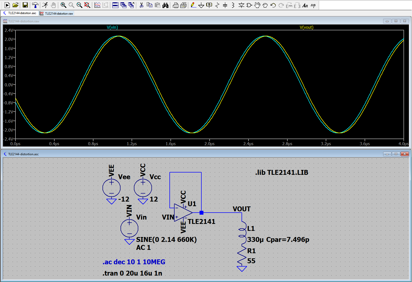
Do not discard the simulation data from consideration: however sound, speaking in general, is disbelieve concerning simulation predictions, I've examined the TI simulation model for TLE2141 and not found any implementation detail (at least those I am aware of) that the developers had missed to include. For the record: in my opinion, the model covering of harmonic distortion is quite trustworthy.

TLE2144-q639414

No visible distortion at all. You may become interested in output current:

TLE2144-q639414-current

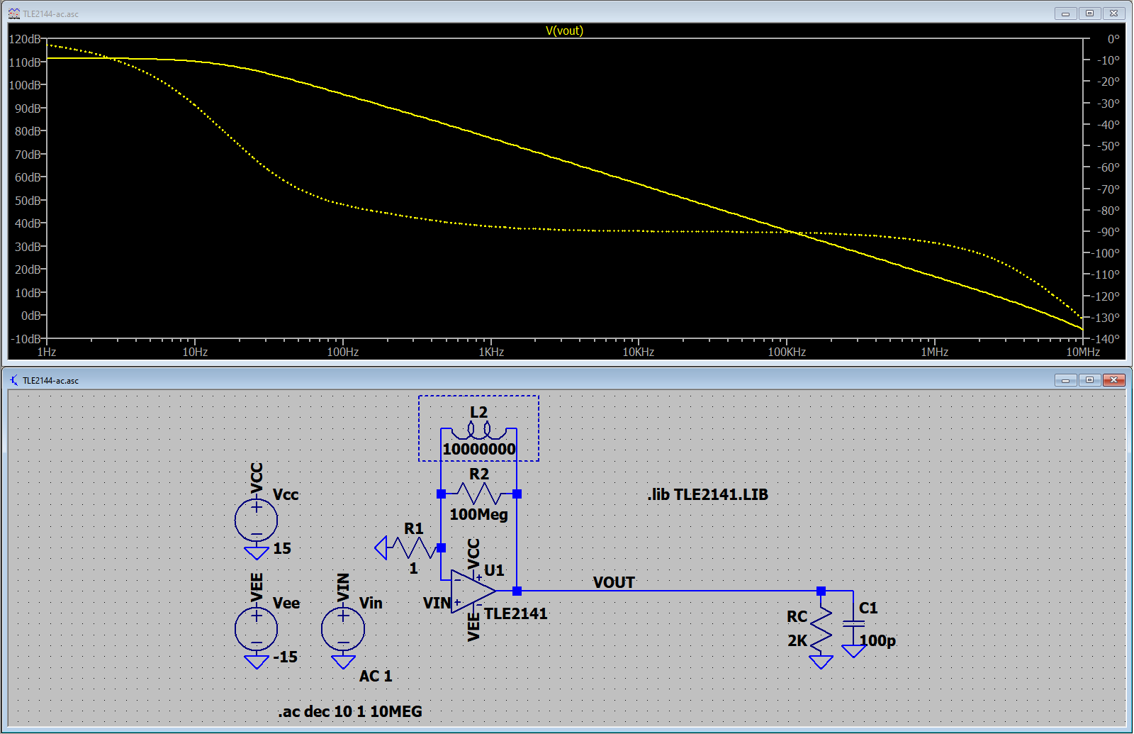
Finally, the .ac analysis simulation run

TLE2144-q639414-ac(fig-15)

gives an \$A_{VD}\$-vs-frequency plot, exactly representing the graph of Figure 15 of the datasheet. The inductor in the opamp feedback is only a technical trick used for the .ac analysis, permits to compute the DC operating point, helps avoid the opamp being sticked to the rail voltage, and has no meaning for the real device operation.

\$\endgroup\$
0
\$\begingroup\$

Using a voltage follower with TLE2144, I was able to get an output of 4.5 Vpp with an input from the function generator, but after it reaches above 510 kHz, the signal starts to distort on the negative cycle.

Unless a "wiring" problem on test board ...

Don't know if this can help, but my simulation does not show distortion until 700 kHz is reached with a peak-to-peak voltage output of 20 V (as OP third graph shows).
Don't know where the "bug" is?

enter image description here

For ~ 5 Vpp, frequency should be 2.5 MHz (?).

enter image description here

\$\endgroup\$
3
  • \$\begingroup\$ i know for sure that it is not wiring issue since it is on PCB. \$\endgroup\$ Commented Oct 24, 2022 at 1:39
  • \$\begingroup\$ Ok. Under "wiring", I mean and I include also all "parasitic" capacitors which are not included in the schematic (example of the "test" points of scope which add at least 5 to 10 pF) ... and not included in the simulator. \$\endgroup\$
    – Antonio51
    Commented Oct 24, 2022 at 17:52
  • \$\begingroup\$ I suggest also making all measures with the circuit in a metal box grounded ... Anything could happen. \$\endgroup\$
    – Antonio51
    Commented Oct 24, 2022 at 18:25
0
\$\begingroup\$

For an op amp to be accurate, its open loop gain at a given frequency should be “infinitely high”. The op amp you’re using has open loop DC gain in the tens of thousands. But at 0.5MHz, the open loop gain is down by more than 3 orders of magnitude. A good follower for a 600kHz signal would need, say, open loop gain of 1000 at 600kHz. The GBW needed is 600kHz×1000=600MHz, not 27MHz!

The load you have is reactive, and some op-amps may not like it even if it is not capacitive. It depends on how the inductor is constructed perhaps.

\$\endgroup\$
0

Your Answer

By clicking “Post Your Answer”, you agree to our terms of service and acknowledge you have read our privacy policy.

Not the answer you're looking for? Browse other questions tagged or ask your own question.