12
\$\begingroup\$

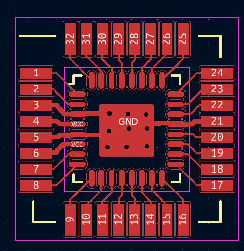
In order to ease supply issues, I am considering an overlapping footprint for the TQFP-32 and VQFN-32 packages of ATmega48/88/168/328 CPUs. The two packages have the same pinout. It's a commercial project, likely to make a few thousand units over a five-year period.

Has anyone tried this successfully? Are there any surprises? Any issue because of the signals going a little under the (larger) part? Any issues in fabrication or placement?

Obviously the alternative is to have to have multiple-version PCBs, with the additional documentation management overhead. This way obviously "wastes" the area under the chip for tracks.

It would look something like this (updated with thermals and GND/VCC):

enter image description here

Additional information in response to comments:

  • The design uses the internal oscillator
  • There are no analogue inputs or outputs
  • Most of the outputs are PWM; also RS485 at 250 or 500 kbit/sec; some i2c.
  • Bottom thermal pad will be connected to GND, with thermal vias, per datasheet p643. Pins 3, 5, 21 are also GND; pins 4 and 6 are VCC. The smaller part has a thermal pad on the bottom, the larger one does not.
\$\endgroup\$
10
  • 2
    \$\begingroup\$ Analog input? Crystal oscillator? These might be adversely affected. Do be careful to terminate un-used pins. \$\endgroup\$
    – glen_geek
    Commented Nov 23, 2022 at 13:39
  • \$\begingroup\$ @glen_geek thank you for your comment, edited question (internal osc, no analogue). \$\endgroup\$
    – jonathanjo
    Commented Nov 23, 2022 at 13:44
  • 7
    \$\begingroup\$ Will you be using two paste masks? I'd be worried about the larger chip sitting on the solder paste deposited on the large QFN center pad and floating up when soldered. But I've never done this, so just hand waving here. \$\endgroup\$
    – bobflux
    Commented Nov 23, 2022 at 14:07
  • \$\begingroup\$ @bobflux that's a very good point, makes me think two masks is a very good idea, most especially when larger package being installed. \$\endgroup\$
    – jonathanjo
    Commented Nov 23, 2022 at 14:26
  • 2
    \$\begingroup\$ @Lundin I meant stencils too, I wrote some Frenglish by mistake \$\endgroup\$
    – bobflux
    Commented Nov 23, 2022 at 15:42

1 Answer 1

14
\$\begingroup\$

Has anyone tried this successfully?

My company does this in current designs because of Chip shortages and not just with this part. There are many companies that are doing this more and more. Or some of the ti buffer chips they can be stacked three times for three different sizes of parts.

One issue you might run into is if the outer part has a thermal pad under the part then that could potentially short pins out. You may have to tell the assembly house of your special condition but most should be able to handle it with just a loading diagram and a change in the BOM.

If there any signals over ~50 MHz you will be adding a very small amount of capacitance with the extra pads so this could affect rise times.

\$\endgroup\$
2
  • \$\begingroup\$ The outer package has no thermal pad on this part; the smaller one does. \$\endgroup\$
    – jonathanjo
    Commented Nov 23, 2022 at 15:11
  • 3
    \$\begingroup\$ I figured, but it was worth mentioning for others \$\endgroup\$
    – Voltage Spike
    Commented Nov 23, 2022 at 15:27

Your Answer

By clicking “Post Your Answer”, you agree to our terms of service and acknowledge you have read our privacy policy.

Not the answer you're looking for? Browse other questions tagged or ask your own question.