5
\$\begingroup\$

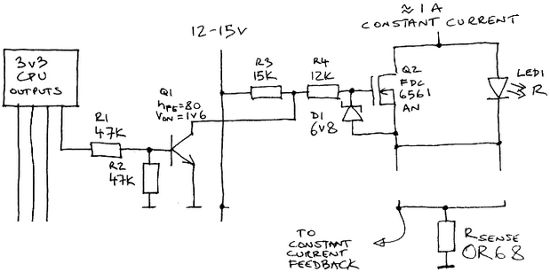
I am designing a commercial LED driver to replace one which is no longer available, and because of supply chain issues I'm trying to select "maximally available/maximally substitutable" parts. The driver is a parallel FET shunt LED driver, made with a stack of four MOSFETs shunting four LEDs under PWM at 1 kHz, under a constant current source of about 0.5 A, perhaps as high as 1 A.

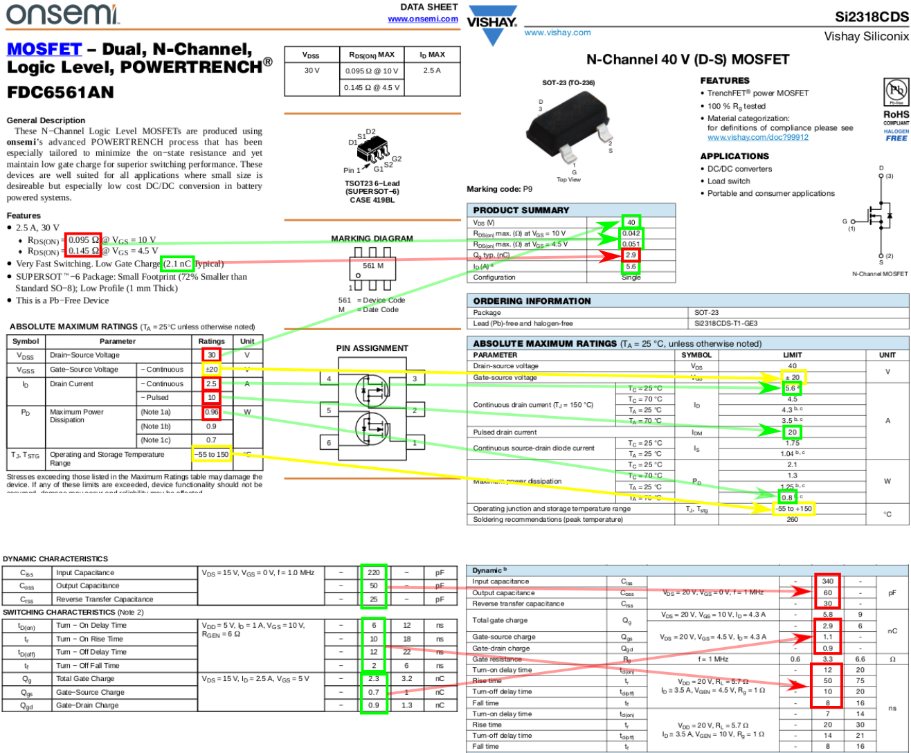
Question: I am considering replacing an FDC6561AN (Q2 in diagram below) with (two) SI2318CDS and have compared their datasheets (see below). My understanding is that for this circuit the most important parameter is RDS(ON), as this controls the power used by the part: when the LED is off, the MOSFET takes the whole current. The old part is 145 mΩ, new part 51 mΩ thus power loss is about a third: excellent. The only parameters which are worse are the gate charge, and various timings, which are higher, but all in same order of magnitude in nC, ns, pF. How important is this? I believe at 1 kHz they are immaterial.

Is this the correct emphasis for MOSFET performance in this kind of circuit?

(Selection criteria were: voltages, currents, thermal better, low RDS(ON); package SOT-23 for many alternatives; good stock at major distributors.)
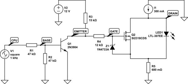
schematic

enter image description here enter image description here


2023-08-03: Update after implementation

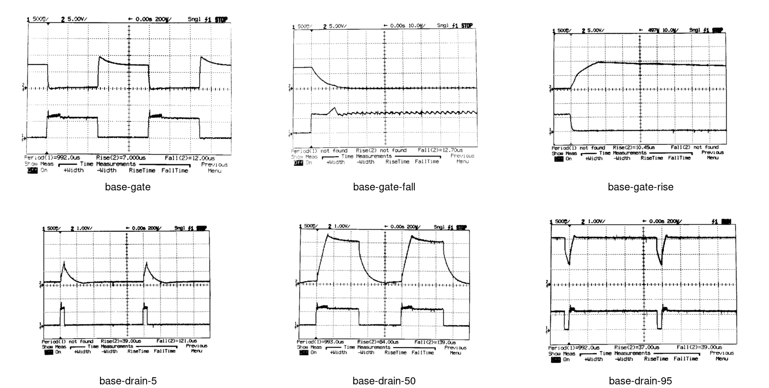
These are scope traces of a built circuit in action: I=300mA, Q1=MMBT3904, Q2=SI2318CD per datasheet above, R1=47K, R2=47K, R3=15K, R4=12K, D1=6V8. It shows pretty much the behaviour anticipated by Tim Williams (slow rise and fall on the gate); and at the drain a 5% duty cycle gives "shark fin"; 95% duty cycle gives "V-notch". enter image description here
\$\endgroup\$
2
  • 1
    \$\begingroup\$ Have you simulated it? \$\endgroup\$
    – Andy aka
    Commented Nov 29, 2022 at 9:41
  • 1
    \$\begingroup\$ @Andyaka thanks for your comment question: I'm in the process of making sense of Vishay's SPICE models. My question is about which parameters of a MOSFET are most important in the design of this kind of circuit. \$\endgroup\$
    – jonathanjo
    Commented Nov 29, 2022 at 10:15

2 Answers 2

7
\$\begingroup\$

At 1kHz, switching loss is essentially irrelevant, even with fairly lax drive. That means switching times (notice the generator resistance RG or RGEN they are specified with) and gate charge are unimportant.

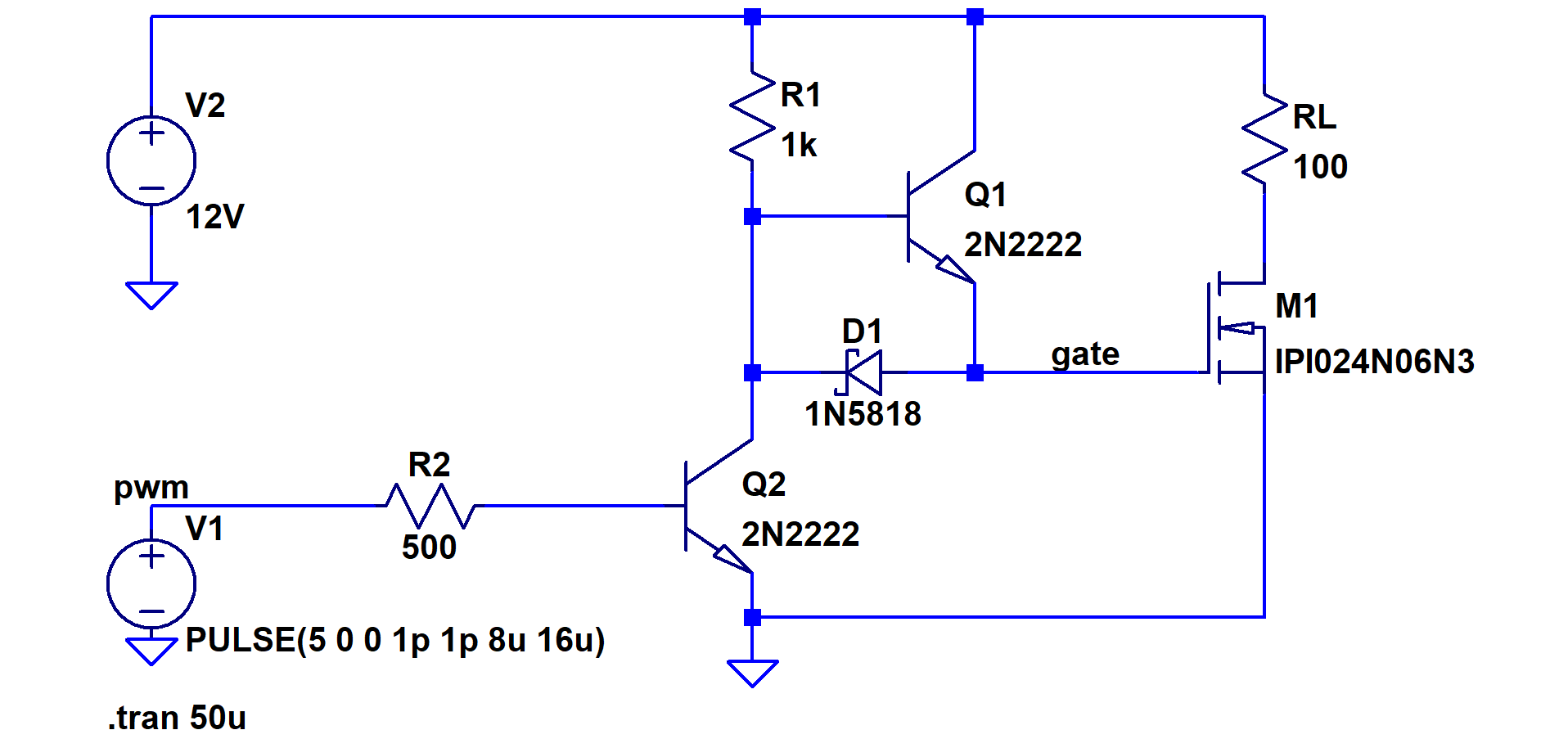
That said, the 12 to 27kΩ drive is ponderously slow, for no obvious reason. Consider a circuit like this:

Gate driver circuit

(Image source: CircuitDen | Artin Isagholian - Discrete Gate Driver Designs, Design 1 (Low Current))

Note that R1 is equivalent to your R3. The zener can be placed on the same node (Q2 collector) to limit gate voltage if needed. The diode (a smaller type like BAT54 or BAT85 can be used) allows Q2 to pull down the gate, discharging faster than a resistor alone, while saving transistor count. (Not that it matters much, transistors are quite cheap.) Meanwhile, Q1 acts to multiply R1's current, by its hFE roughly, thus a 10k pullup looks like ~100Ω to the gate.

I'm guessing low current consumption isn't much of a problem, given the shunting mode output, so additional savings aren't really necessary. If they were, options would include CMOS level shifters/drivers, reevaluating the current source (use a lower sense voltage? use a more efficient SMPS?), and perhaps using power-saving modes in the MCU and any other peripherals (most of these being well beyond the scope of this particular question).


Edit: another example for the "it pays to actually calculate" bin!

The gate voltage rise/fall is quite slow. Qg(tot)(max) = 3 or 6nC at 5V, respectively. The gate is a nonlinear capacitance, but we can approximate it as an average equivalent by simply dividing total charge by the voltage swing. This gives 0.6 or 1.2nF average gate capacitance Ciss(avg).

Against 12k (falling) or 27k (rising), that capacitance will have a time constant of 7.2 to 32.4µs. Versus a ~500µs half-period at 1kHz -- and worse for any duty cycle other than 50%, that's a fairly large amount of time spent in the transition.

Now, the full risetime (10-90%) will be about 2.2 times the RC time constant, but also, the bulk of the actual switching occurs in a fraction of this -- about QGD, or for these transistors, about a third of the total. So it's not quite as bad as it sounds, but it also means there will be distortion (actual pulse width at the LEDs different from what's driven) near the extremes, as the on or off period approaches this time. So, for duty cycles outside of say 10-90%, it's not looking great.

Using a 10k pullup with hFE = 100 follower would give a modest rise of 100-200ns, just fast enough to be worth checking out EMI, and more than fast enough to give a reasonable duty range.

The pull-down transistor (Q2 above, Q1 in the original) should be driven hard enough to pull down the gate in reasonable time; not much static pull-down is needed, but a series resistor and capacitor can be wired in parallel with your R1, say 220R + 2.2nF, to greatly increase turn-on current without increasing DC consumption. (A discharge path will also be needed: connect a signal diode (BAT54, BAT85, 1N4148, etc.) from GND (anode) to Q1 base (cathode) to do this.)

\$\endgroup\$
9
  • \$\begingroup\$ Many thanks for your suggestions. When you say "the 12 to 27kΩ drive is ponderously slow, for no obvious reason." Do you mean it's not clear why the circuit has it, or it's not clear why it is slow? Can I ask too what part you mean is slow? \$\endgroup\$
    – jonathanjo
    Commented Dec 2, 2022 at 18:56
  • \$\begingroup\$ @jonathanjo See edit. \$\endgroup\$ Commented Dec 2, 2022 at 20:03
  • \$\begingroup\$ many thanks for further explanation, I'll put a scope on the running circuit and see if it matches prediction. (Just to be clear: I should look at the slope of the Q2 gate?) \$\endgroup\$
    – jonathanjo
    Commented Dec 2, 2022 at 20:11
  • \$\begingroup\$ This is a great answer. \$\endgroup\$ Commented Dec 2, 2022 at 21:20
  • \$\begingroup\$ @TimWilliams I posted scope traces of a built circuit, if you had a moment I'd be very interested to read any comments you might have for the "it pays to actually measure" bin. \$\endgroup\$
    – jonathanjo
    Commented Aug 3, 2023 at 16:47
4
\$\begingroup\$

Basically, switching losses increase with increased total gate charge and increased switching frequency. Gate drive losses, which is part of switching losses, can be described as

$$ P_g=Q_g \ V_{GSpk} \ f_{SW} $$

where \$Q_g\$ is the total gate charge, \$V_{GSpk}\$ is the peak voltage of gate drive pulses, and \$f_{SW}\$ is the switching frequency.

Lower total gate charge brings lower switching losses as well as faster switching. But these parameters are more meaningful in applications where the load currents reach a few amps or more, and the switching frequencies are a few tens to a few hundreds of kHz.

In your case the gate drive losses don't reach to mW values, also the switching frequency is 1 kHz so there's nothing to worry about with the MOSFET's parameters.


One thing to consider here is the input capacitance, \$C_{iss}\$. Although the gate-source thresholds for these MOSFETs are relatively low, with the existence of relatively high gate stopper resistors (R3+R4 for turn on, R4 for turn off) the input cap's contribution to rise and fall times becomes more of a concern. Since these times basically determine how long the MOSFET stays in ohmic (linear) region, increasing these times will obviously increase conduction losses (Remember that the gate stopper resistor(s) and input capacitance of the MOSFET form a RC filter which brings a turn-on and turn-off delay). Note that the turn on and rise/fall times in the datasheet are given for a gate stopper resistor of 6 Ohms. In your case, this resistor is 27k for turn on and 12k for turn off. So the cut-off frequency of the formed filter can be as low as 17 kHz which doesn't seem to be a serious problem for 1 kHz operation (or 500 us of on and off times). But this is always a thing to consider.

I understand that these resistors cannot be easily decreased due to the existence of small signal transistor which has relatively low collector current ratings. This design may not be a problem for 1 kHz operation but can be a serious one for higher switching frequencies.

\$\endgroup\$
1
  • \$\begingroup\$ Many thanks for your answer. To clarify, the 1 kHz PWM has variable duty cycle from 1/255 to 254/255, as well as DC 0 and DC 3v3. If you had advice on suitable C<sub>iss</sub> I should look for I'd be very grateful. The small signal transistor at the front is likely to change to 2m3904. \$\endgroup\$
    – jonathanjo
    Commented Dec 2, 2022 at 19:00

Your Answer

By clicking “Post Your Answer”, you agree to our terms of service and acknowledge you have read our privacy policy.

Not the answer you're looking for? Browse other questions tagged or ask your own question.