1
\$\begingroup\$

I'm using an NSR006A0X4Z DC/DC with 12V input and set to produce 2.5V output (Rtrim = 619Ω).

This is used for a current source, controlled by GPIOs of a Raspb Pi: enter image description here
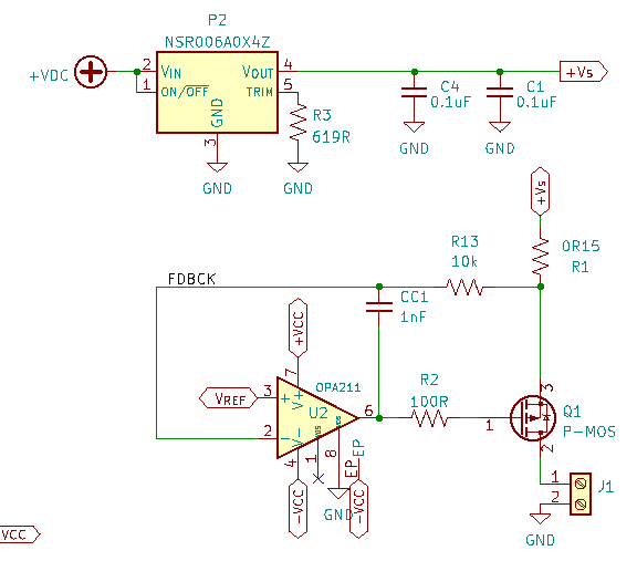
The op-amp is powered with ±5V. The output (power) transistor is the SPP80P06P H, with a Vthreshold of 4V max (well, ‒4V, being p-channel).

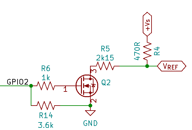
VREF is generated through the GPIOs; the following is a simplified version of it:

enter image description here

With GPIO2 at 0, VREF = Vs, which I confirmed is 2.5V (well, 2.498V according to the multimeter), and this produces an output current of 0A. When setting GPIO2 to 1, VREF is supposed to be set at 2.05V, producing an output current of 3A.

However, the output current is lower (approx. 2.76A) because Vs drops to approx. 2.43V.

The "upstream" power source (+VDC in the schematic) comes from a wall adapter that specifies an output of 12V / 3.6A max.

The only detail the NSR006A0X4Z datasheet says that could explain is the external output capacitor, which as they put it, "reduce the output ripple and improve the dynamic response to a step load change". Since I am "instantly" (well, as instantly as the circuit allows) switching from 0A to 3A, I thought that might be it. I added a 100uF/16V Aluminum Polymer capacitor at the output (soldered it right at the converter's output pin, with the other pin soldered to a ground plane copper pour). No change.

The behavior seems consistent; not only have I tried two different boards and observed essentially identical results; one of the boards originally had the OKR-T-10-W12, and we switched to the NSR006A0x4Z because the OKR went out-of-stock. But the issue was essentially identical with the OKR-T-10-W12 (albeit, the board that had the OKR never had the 100uF capacitor at the output).

Any ideas why?

\$\endgroup\$
7
  • 2
    \$\begingroup\$ Have you measured the output of the regulator right across the output pin and ground pin at the device? It doesn't have a provision for remote sense, so it can only regulate right at the output and ground. \$\endgroup\$
    – John D
    Commented Dec 16, 2022 at 19:16
  • \$\begingroup\$ Interesting suggestion; I will check it, however, I doubt I'll find any surprises; Vs only goes to those two places in the schematic, and the trace connecting them is about 25mm long, 1.5mm wide (1-oz thickness). Plus, the 470Ω resistor that connects to Vs is less than 5mm away from the regulator's output pin, and I'm pretty sure I measured the voltage there and it was lower. \$\endgroup\$
    – Cal-linux
    Commented Dec 16, 2022 at 19:30
  • 2
    \$\begingroup\$ If 2.786A is flowing through R1 (0.15Ω), then there should be 0.4152V across it - could you confirm please. \$\endgroup\$
    – rdtsc
    Commented Dec 16, 2022 at 19:49
  • 2
    \$\begingroup\$ Huh ... I'll be dammed ... Measuring between the pads of the decoupling cap (about 2mm away from the regulator's pins), I get a drop from around 2.498 to 2.486, but measuring at the 0.15Ω resistor pin, it drops to 2.457V. That actually goes with the resistance of the trace! (it's about 8mΩ as per the allaboutcircuits trace resistance calculator), so that means a drop of about 24mV. I failed to realize that the circuit relies on somewhat small voltage variations to determine the current, so the normally-negligible drop due to the trace resistance is not-really-negligible in this context! \$\endgroup\$
    – Cal-linux
    Commented Dec 16, 2022 at 20:03
  • 1
    \$\begingroup\$ The drop on the actual voltage (measured right next to the regulator's pins) is actually non-negligible: 12mV !! I guess it's not a matter of using a thicker trace or placing the regulator right next to R1's pin, but rather using a regulator with "remote sensing" (Kelvin connection, I believe it's called?) \$\endgroup\$
    – Cal-linux
    Commented Dec 16, 2022 at 20:10

2 Answers 2

2
\$\begingroup\$

Formulating an answer based on comment from John D, plus the follow-up investigation/debugging on my side:

The DC/DC converter output is not dropping (in any case, no more than what the manufacturer specifies — load regulation, etc.); the trace resistance from the regulator's output pin to the R1 pin is about 8 ~ 10 mΩ, making R1 effectively 0.16Ω instead of 0.15Ω; that's about 7% change, explaining the ~ 8% change that I measure.

One fix is: since the 470Ω resistor used to generate the Vref is right next to the regulator's output, its voltage there is very close to the nominal Vs = 2.5V, so Vref is correctly generated; it's simply a matter of acknowledging the new value of R1 = 0.16Ω and adjusting R4/R5 to produce the required Vref.

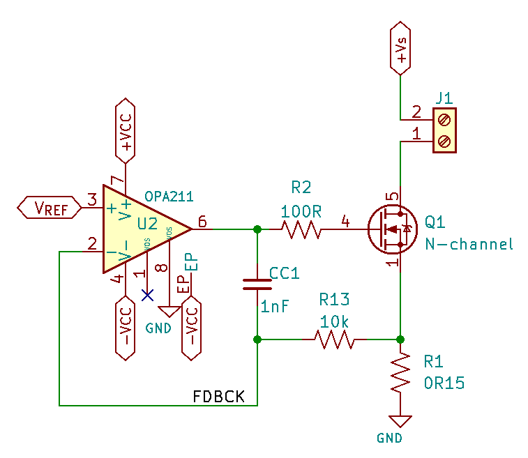
If redesigning, instead of redoing the layout with either a very thick trace, or a power plane, or placing the regulator right next to R1, it would make sense to place R1 on the low-side, and use an N-channel transistor (which is advantageous anyway): enter image description here

Because the ground connection is typically more solid (I have ground copper pours on both top and bottom layers), then the issue will be much less significant. Plus, this circuit configuration does not prohibit the additional change of placing the regulator close to R1 anyway.

Here, the Vs connecting to J1 can be subject to drop under load, because the op-amp+Q1 provide the negative feedback to regulate the current (provided that Vs at J1 does not drop so much that it would drive the op-amp outside of linear operation).

Thanks to John D for noticing and pointing out the key detail !

\$\endgroup\$
1
  • 1
    \$\begingroup\$ You could also, if the drop due to R1 is too much, consider using a hall-effect sensor like an ACS723. \$\endgroup\$
    – Hearth
    Commented Dec 19, 2022 at 13:58
0
\$\begingroup\$

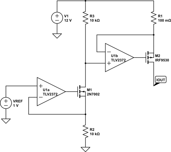
You can duplicate the circuit upside-down to level-shift it to a less stable supply:

schematic

simulate this circuit – Schematic created using CircuitLab

Resistor values just for example. Also, compensation not shown; the way you have it is fine (or, with CC1 with a resistor in series -- evaluate step response for best results).

\$\endgroup\$
2
  • 1
    \$\begingroup\$ That's the approach I'd recommend. It's cheap and performs quite well. The mosfets have enough gate-drain capacitance to stabilize the op-amp, usually. The connections to R1 should still be Kelvin of course! Nothing can work around that. \$\endgroup\$ Commented Dec 19, 2022 at 20:28
  • \$\begingroup\$ @Kubahasn'tforgottenMonica Yes, good point: to be precise, R3 needs to be common to R1's reference terminal on that side. \$\endgroup\$ Commented Dec 19, 2022 at 22:13

Your Answer

By clicking “Post Your Answer”, you agree to our terms of service and acknowledge you have read our privacy policy.

Not the answer you're looking for? Browse other questions tagged or ask your own question.