2
\$\begingroup\$

I am creating a footprint for a 24-pin QFN package with exposed thermal pad. Sometimes manufacturers will provide solder paste mask guidelines in addition to metallization for the landing pattern, but not always.

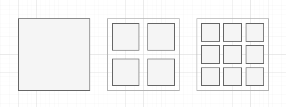
I believe I need to reduce solder paste deposition by about half, but I am wondering how large gaps between openings need to be, and what size and how many smaller openings to create:

Solder mask windowing options

My questions then are:

  1. Should I leave the solder paste opening the same size as the copper pad (default) and let our fabricators do their own reduction (as I've been told they sometimes do)?

  2. Should I create "windowed" solder paste openings and if so, what guidelines are recommended if the manufacturer does not provide them?

(The exposed pad size is 4.8 mm2 but I am asking more for the general case rather than this specific component.)

\$\endgroup\$
2
  • 2
    \$\begingroup\$ So if its standard 24 4x4 QFN or 5x5 just use the parametric search on mouser/digikey and scan different datasheets for advise. Or go to one of the major IC-manufacturers (TI, Maxim, NS, etc. ) website and browse their documentation - usually they will allow searches for specific package-types. Or ask your assembler. They will know and maybe even have detailed drawings/recommenations based on real-world experience. \$\endgroup\$ Commented Dec 21, 2022 at 23:10
  • \$\begingroup\$ @ElectronicsStudent That's what I usually do for standard packages, but I asked the question because I wanted to know if there are guidelines when such options aren't readily available. (Granted, that's not often, but I am still curious.) \$\endgroup\$
    – JYelton
    Commented Dec 21, 2022 at 23:34

3 Answers 3

3
\$\begingroup\$

I need to reduce solder paste deposition by about half, but I am wondering how large gaps between openings need to be

The goal is to approximate a 50% density halftone screen. Think of the little dots used to print grayscale with black ink on paper, except this is using solder paste on a PCB.

To a first approximation, the gaps need to be such that the opening area you leave is 50% of the pad area. This is basic geometry, then. The area of the gaps needs to add up to 50% of the pad area. Easy to calculate.

Then, there is a tradeoff between the number of openings and the accuracy of deposition: the smaller the openings, the larger the relative paste volume error. Solder paste printing is not an exact process, and each unit length of the boundary of the opening introduces a certain fixed excess/shortfall of paste.

The number of openings needs to strike a balance between the even adhesion of the chip to the PCB - facilitated by numerous paste "dots", vs. the limitations of the printing process.

Should I leave the solder paste opening the same size as the copper pad (default) and let our fabricators do their own reduction (as I've been told they sometimes do)?

Ask the fabricator! They must be explicit about whether they change anything on your submission or not.

  1. Should I create "windowed" solder paste openings and if so, what guidelines are recommended if the manufacturer does not provide them?

The guidelines should come from the board assembly house that handles stencil making and paste printing.

As long as you are sure about the need of 50% paste volume reduction needed, relative to the thermal pad area, then it's a simple matter of geometry to cover 50% of the pad's area with paste. The choice you have is reduced to just one: into how many openings should the paste be split into. You have not told us how large the thermal pad is. I usually keep the opening size above 50x50 mils for larger pads, and 30x30 mils for smaller pads. There's quite a bit of leeway here - a range of grid counts (columns/rows) will usually provide similar results. Ask the FAB house for details!

\$\endgroup\$
1
  • \$\begingroup\$ I added the pad dimensions for reference (4.8mm^2) but I don't want to limit answers to that specific pad size. Thanks for the info so far. (I worked in professional offset printing for over a decade so am very familiar with halftone! But a stencil wouldn't release solder paste if we were to create fine meshes of dots like that, I presume!) \$\endgroup\$
    – JYelton
    Commented Dec 22, 2022 at 1:17
1
\$\begingroup\$

From what I can see there are only the most general guidelines in IPC-7525. A reduction to 50%-80% is recommended onto the ground plane via window paning, and it is recommended that any vias be positioned under the web so as to minimize solder wicking.

\$\endgroup\$
0
\$\begingroup\$

This question was posed a few days ago in this discussion.

An interesting reference was to Texas Instruments' AN-1187 which discusses percentage of solder fill for the thermal paddle. Tables 3 & 4 are relevant to your question.

\$\endgroup\$
1
  • \$\begingroup\$ This is basically a link-only answer. Could you please briefly summarise the relevant points of the documents you linked? \$\endgroup\$
    – TooTea
    Commented Dec 22, 2022 at 7:18

Your Answer

By clicking “Post Your Answer”, you agree to our terms of service and acknowledge you have read our privacy policy.

Not the answer you're looking for? Browse other questions tagged or ask your own question.