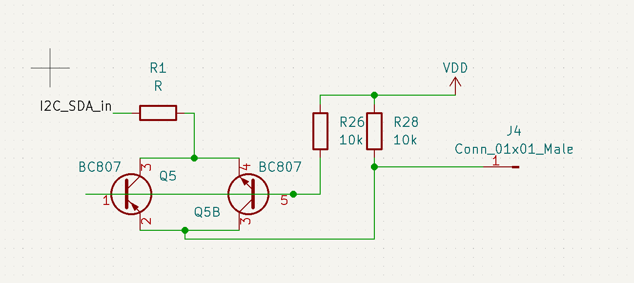
If the other device has the pull-ups then you can use the following:

simulate this circuit – Schematic created using CircuitLab
NOTE: Shown for SDA only, so you should duplicate this for SCL.
TRANSMISSION FROM YOUR SIDE
- When SDA (SCL) is high the MOSFET will be off (because gate-source voltage is zero), so the SDA (SCL) on the other side will see high through its internal pull-up.
- When SDA (SCL) is low the MOSFET will turn-on (because gate-source voltage becomes positive, 1.8V) and shorts the SDA (SCL) line on other side to ground, so it'll see low.
TRANSMISSION FROM OTHER SIDE
- When SDA (SCL) is high then nothing changes i.e. this is the initial state, so no switching happens. So SDA (SCL) on your side will see high through pull-up.
- When SDA (SCL) is low the body diode of the MOSFET will conduct, so the SDA (SCL) on your side will see a diode drop initially. This will make the gate-source voltage positive, then the MOSFET turns on and shorts the diode, making the voltage seen from your side zero.
The main problem here is to find an NMOS with really low threshold gate-source voltage. 2N7002 is quite common and considered as logic-level-gate MOSFET but its VGS-th can be as high as 2V so it's not suitable. This can be used as it has 2 NMOS inside (one for SDA, one for SCL) with very low input and output capacitances (This is not an advertisement). Or you can check global distributors (e.g. Digikey, Mouser) for other options.


