11
\$\begingroup\$

I am confused about several aspects pertaining to op-amp DC biasing and its effects on ground/common mode limits. The more I read about this, the more muddled up I get. I will try to frame my queries as coherently as possible and would really appreciate it if you could address them all.

My first question is related to an op-amp's inner reference/ground. I have gone through the following threads:

Confused about opamp's inner "ground"

What Reference-Potential does an Operational Amplifier use as "Ground"-Potential?

How does an op-amp know where ground is?

What Reference-Potential does an Operational Amplifier use as "Ground"-Potential?

Although some information seems to be conflicting (https://electronics.stackexchange.com/a/534783/286984: this answer states the ground is mid-point of supply, where as https://electronics.stackexchange.com/a/405898/286984 states it is the negative supply), one thing they have in common is that both state that ultimately it doesn't matter because of the feedback which references it to the input's ground.

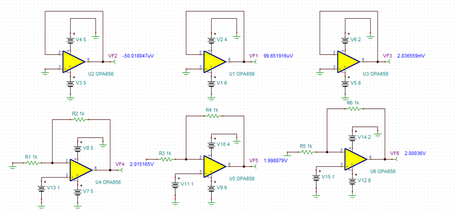
However, if that is the case, no matter what input I give an op-amp, the output should remain same with respect to the input's ground. I simulated the following conditions where I am shifting supply, and I am seeing a change in the output. What is the reason for this? Has my reference shifted somehow?

enter image description here

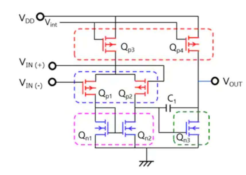
As I fell deeper into the rabbit hole, I started looking at a differential pair and further questions arose. Consider the following circuit:

enter image description here

The output would need to be centered around a DC bias point equal to (VDD-VGS(QP4)) with respect to VEE (negative supply). How does this DC voltage not show up at the output of op-amp?

Also looking at the differential pair, it seems that everything should be referenced to VEE, however, my simulation results above suggested the mid-supply seems to be some sort of reference.

So there does seem to be some internal reference at play: mid-supply or input voltage or some magic, so I don't know why so many answers I linked seem to say it doesn't matter. Please clarify, once and for all, what is the op-amp's reference?

\$\endgroup\$
1
  • 2
    \$\begingroup\$ There's no constructed internal "virtual ground" that sits halfway between the opamp rails. The opamp just has the two rails to work from. \$\endgroup\$ Commented Feb 1, 2023 at 20:50

6 Answers 6

5
\$\begingroup\$

So, there does seem to be some internal reference at play: mid-supply or input voltage or some magic, so I don't know why so many answers I linked seem to say it doesn't matter. Please clarify, once and for all, what is the opamp's reference?

Once and for all, "There is no reference".

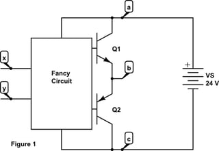
FIgure 1 below shows a crude model of an operational amplifier. The lowercase letters are the names of the accessible nodes. Notice that no reference node is specified or indicated. This makes it impossible to talk about the voltage \$V_a\$ for example or any of the other nodes using single subscript notation. However, without knowing the voltage at a reference node, the quantity \$V_{ac}=V_a -V_c\$ can easily be determined as 24V, as long as the same reference is used even if the voltage there is unknown. The fact that \$V_{ab}\$ is positive can also be determined.

schematic

simulate this circuit – Schematic created using CircuitLab

So how does this crude operational amplifier work. First the voltage \$V_D =V_{xy}= V_x-V_y\$ is defined. This allows us to have a known voltage from \$x\$ to \$y\$ even if the actual voltages \$V_x\$ and \$V_y\$ are unknown (because there is no reference).

The two transistors can be considered variable resistors. Let's call them \$R_{Q1}\$ and \$R_{Q2}\$.

Symmetry of \$Q_1\$ and \$Q_2\$ can be used to argue that the collector-emitter voltage drops of the two transistors are equal and opposite: \$V_{ab}=-V_{cb}=12V\$. In fact the first specification for the op-amp is:

1. If \$V_D=0\$ then \$V_{ab}=V_{bc}\$.

The second specification is:

2. If \$V_D\$ increases above zero then \$R_{Q1}\$ decreases and \$R_{Q2}\$ increases and vice versa.

The third specification sets how sensitive the operation is:

3. If \$V_b\$ (relative to an arbitrary reference) increases by 1 volt, then \$V_D\$ will be \$\frac{1V}{A_V}\$, such that the change in \$V_b\$ is: $$\Delta V_b=A_V V_D.$$

The preceding has been developed without the need for a known reference.

Here is the revelation. A specific input voltage \$V_D\$ produces a defined change in the output. This is an open-loop characteristic in that it is designed-in and calibrated. The input does not "know" that the output does anything. An absolute input value will not produce specified absolute output unless the system is linear.

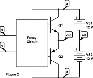
Now lets introduce an external reference voltage. It is still unknown so \$V_{ref}\$ can be used to represent it. The voltage at node b can be written: $$V_b= \Delta V_b+V_{ref}=A_vV_D+V_{ref}\tag{1}$$

So if \$V_{ref}\$ is unknown how is ithat we can know what it is. Well--- we get to choose it. That is the only way to "know" what the reference voltage is. To linearize Equation 1, \$V_{ref}\$ should be 0V. But what does that mean.

Remember the symmetry argument that for \$V_D=0V\$, \$V_b\$ is midway between \$V_a\$ and \$V_c\$. If a known mid point voltage source is created externally to the op-amp, then a voltmeter, placed from \$V_b\$ to the now known \$V_{ref}\$, will read 0V.

schematic

simulate this circuit

All that is left is to rename \$V_b\$ as \$V_{out}\$. So Equation 1 is now linear: $$V_{out}=A_vV_D$$

The linearization is important for measurements to make sense, and to tranfer meaningful voltages from one circuit to the next.

Additional point: The operational amplifier still has no reference. It does not "know" that there are two 12 volt sources. It does not "know" that the reference point exists. The reference is purely for our needs and sensibilities; for use where implementing circuitry using the operational amplifier in its various closed loop forms.


common mode dependence on supply

I simulated the following conditions where I am shifting supply, and I am seeing a change in the output. What is the reason for this? Has my reference shifted somehow?

Yes the reference is changed. When the input voltage \$V_D=0V\$,\$V_{out}\$ is at the midpoint voltage. The common mode input voltage will not change that (by design). You changed the reference from the midpoint so the measured output will reflect the reference change. The circuit is no longer linear.

The output would need to be centered around a DC bias point equal to (VDD-VGS(QP4)) with respect to VEE (negative supply). How does this DC voltage not show up at the output of opamp?

When the input voltage \$V_D=0V\$,\$V_{out}\$ is the midpoint voltage (also by design). And yes the voltage does appear at the output. Choosing the reference voltage to be equal to the midpoint as discussed above essentially treats that voltage value as zero volts.

Even single supply op-amps need to be reffered to a mid-point bias reference that some call a virtual ground. (It is different from the input virtual ground of an op-amp.) The FETs: \$Q_{P3},Q_{P4},Q_{N2}\$ in the OPs diagram are current sources that serve to remove dependance on any reference or supply rails.

\$\endgroup\$
5
\$\begingroup\$

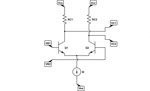
Just focus on the BJT differential pair -- easier to explain:

schematic

simulate this circuit – Schematic created using CircuitLab

The differential pair, \$Q_1\$ and \$Q_2\$, split \$I_{_\text{E}}\$ between them. If \$V_{_{\text{B}_1}}=V_{_{\text{B}_2}}\$ then the split is 50:50. It doesn't matter if \$V_{_{\text{B}_1}}=V_{_{\text{B}_2}}=+2\:\text{V}\$ or if \$V_{_{\text{B}_1}}=V_{_{\text{B}_2}}=-2\:\text{V}\$. If they are both the same, then the current is split equally and therefore the voltage drop caused across \$R_{_{\text{C}_1}}\$ and \$R_{_{\text{C}_2}}\$ are identical and therefore \$V_{_{\text{C}_1}}-V_{_{\text{C}_2}}=0\:\text{V}\$. Or, "No output."

Do you see an internal reference anywhere? I don't.

So long as \$V_{_{\text{B}_1}}=V_{_{\text{B}_2}}\$ their exact voltage doesn't matter. One requirement here is that the current sink, \$I_{_\text{E}}\$, has to have enough voltage headroom (from emitters to \$V_{_\text{EE}}\$) that it can maintain it's "current sink" behavior. Another requirement here is that the collectors of \$Q_1\$ and \$Q_2\$ cannot be forced below their two respective base voltages (or else the dreaded 'saturation' occurs.)

So there are a few limitations. But within those limitations, the two base voltages are free to move about.

The key here is that if there is any difference in the two base voltages, then this is exponentially magnified by the BJT-pair in such a way that the current diverts very rapidly to the collector of the BJT with the higher (more positive) base voltage.

The base voltages are really just voltage differences. It doesn't matter if both base voltages are "with reference to some external circuit ground" or "with reference to the negative rail". When the base input voltages are the same, the output difference is zero. Otherwise, the output difference isn't zero.

In the case of BJTs (not FETs), the allowed difference cannot usually exceed about \$100\:\text{mV}\$ before the point is reached where almost all of the current is taken up by just one of the BJTs. More than that means very little change in the voltage difference at the collectors. So it does reach a point where further differences at the two bases no longer matters much, anymore.

But again, there's no need for an internal reference. That's one of the really nice things about differential pairs like this.

The above circuit isn't actually ever really used, in practice. Not anymore. The current sink needs to work about the same regardless of the two voltage rails, so there is some trickery going on to make that work really well inside most IC opamps. Also, using resistors in the collectors is really poor practice. Those two resistors are almost always replaced with a current mirror, with only one collector used on the side that will squirt current towards another stage that will use it. That's because it's a better arrangement with higher gain and because it's cheaper and takes less space in the IC, as well. So the above example is more just a way to "get the right idea."

The two rails are there to provide a compliance voltage range for the output and a range (after some overhead is accounted) within which the inputs may move together.

\$\endgroup\$
5
\$\begingroup\$

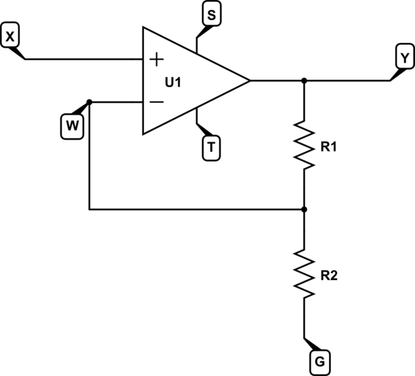
As an example, a typical op-amp based non-inverting amplifier, the way we are usually taught about how it works generally uses assumptions about extremely high open loop gain, and negligible so-and-so, zero this, or infinite that.

At some point in the derivation of gain there may appear an idea of some "reference potential" such as "ground", but strictly speaking that's merely one of many potentials present in the system:
schematic

simulate this circuit – Schematic created using CircuitLab

If we ignore what any of these potentials actually mean, and concentrate only on how we expect an ideal op-amp to respond (at Y) to potentials at X and W, we get a conveniently simple set of equations that we can combine to derive the overall relationship between potentials at X and Y.

For example, the potential \$V_W\$ is somewhere between \$V_Y\$ and \$V_G\$:

$$ V_W = V_G + (V_Y-V_G)\frac{R_2}{R_1+R_2} $$

We also have the ideal op-amp behavior, where A is its open-loop gain:

$$ V_Y = A(V_X-V_W) $$

When you combine these equations, and make the assumption that \$A\$ is very very large and positive, \$A\$ disappears from the equations and you get something like this:

$$ V_Y - V_G \approx (V_X-V_G)\left(1+\frac{R_1}{R_2}\right) $$

Note the "approximately equals" symbol; this is not exact, because A is not infinite in reality. Already we've lost precision.

Note also that we haven't yet declared what \$V_G\$ means, but you can see where I'm going here, because I chose the letter G, short for ground. This circuit behaves as it does, not because there's any "reference potential" anywhere, but purely because that's what the maths says it should do. All the voltage terms in this equation are potential differences, \$V_{SOMETHING}-V_G\$, and if we declare (arbitrarily) that \$V_G=0\$, the algebra simplifies to the familiar relationship for a non-inverting amplifier:

$$ V_Y \approx V_X \left(1+\frac{R_1}{R_2}\right) $$

So, by declaring that \$V_G\$ is our reference "zero" potential, we've got ourselves a super-simple equation, but we mustn't forget that the previous equation containing \$V_G\$ is still valid, and approximately true, and is (technically speaking) more general.

In other words, however we build our op-amp, it needs no knowledge of where zero is, it will always do \$V_Y - V_G \approx (V_X-V_G)\left(1+\frac{R_1}{R_2}\right)\$, and it's only because we arbitrarily choose \$V_G\$ to be zero that it appears as if the op-amp knows where zero is. It doesn't. In fact, it doesn't even know what \$V_G\$ is in this example, since there's no direct connection to the op-amp from \$V_G\$.

--edit 1--
Remembering that the op-amp doesn't have any idea of a "reference", no clue what "zero" actually means, even if it decides to add some ridiculous offset to its output (say 10V), so that the relationship: $$ V_Y = A(V_X-V_W) $$ becomes in reality: $$ V_Y = A(V_X-V_W) + 10 $$ The term \$A(V_X-V_W)\$ is still so large compared to \$10\$ that we may still make this approximation: $$ A(V_X-V_W) + 10 \approx A(V_X-V_W) $$ Thus we may ignore that errant offset, further illustrating why, algebraically, the op-amp's ignorance of zero (or any absolute reference potential) makes little difference to its behaviour when negative feedback is at work.
--/edit 1--

We're not done yet, though, because I still haven't answered why variations in \$V_S\$ or \$V_T\$ (with respect to \$V_G\$) would cause \$V_Y\$ to vary at all.

To understand that, first remember that we made an assumption about \$A\$ being huge, which enabled us to make \$A\$ disappear from the equations. It's not the only assumption we made about \$A\$. We also assumed \$A\$ is constant, and it most definitely is not. We removed \$A\$ from the equations for convenience, but in reality it is still in there playing a role. The hope is that it's always large enough that even significant changes in \$A\$ (say, by a factor of 2) will produce no appreciable change in output, but there will still be some change, never-the-less.

It's impossible to make a differential amplifier, using real-world transistors and other components, that guarantees a constant open-loop gain regardless of how near or far inputs \$V_X\$ and \$V_W\$ are from supplies \$V_S\$ and \$V_T\$. Op-amp designers go to great lengths to get as close as possible to this ideal behaviour, using constant current sources and current mirrors in their long-tailed pairs, but in the end, the truth is that A is not constant, it's a function of all other potentials, and really should be written \$A(V_S, V_T, V_X, V_W)\$. It is always huge, but it varies quite wildly as potentials at the op-amp's various pins change with respect to each other.

An extreme example of \$A\$ changing is when the difference \$V_X-V_W >> 0\$, causing op-amp output Y to saturate; in that case open loop gain \$A\$ drops to zero, and the approximation \$V_Y - V_G \approx (V_X-V_G)\left(1+\frac{R_1}{R_2}\right)\$ fails completely.

The approximation remains true, however, as long as A is still huge, but it's still only an approximation. Variations in \$V_S\$ and \$V_T\$ with respect to \$V_G\$ will cause changes in \$A\$ (and other parameters, I'll mention below), which will result in \$V_Y\$ changing somewhat, as you have seen in your experiments, but the hope is that this effect be negligible.

There are other things that are not constant. Input bias current changes with variations in \$V_W\$, \$V_X\$, \$V_S\$ and \$V_T\$. So does input offset voltage, to a small degree. Any change anywhere causes changes everywhere else, to some degree, but the approximation \$V_Y - V_G \approx (V_X-V_G)\left(1+\frac{R_1}{R_2}\right)\$ remains true.

\$\endgroup\$
4
\$\begingroup\$

For an ideal op-amp, the supply voltage is irrelavant. It does not care what the input is referenced to. It purely amplifies the the voltage difference at its inputs. If the op-amp is part of a feedback amplifier (it always is!) then the the feedback network just steers the output to whatever value is required to equalize the voltage at the inputs of the op-amp. What the 'reference' voltage is, is ultimately determined by the feedback network. For an inverting amplifier for instance, it is easy to see that's the voltage conected to the non-inverting input.

By comparison, a real op-amp will also experience an effect from its supply voltage. This is what you are seeing. In datasheets, this is referred to as the power supply rejection ratio (PSRR). A PSRR of, say, -60 dB, means that a 1V change in power supply voltage is equivalent to a 1 mV change in differential input voltage.

The reason for the finite PSRR is that both inputs are not exactly equal. Perhaps one of the transitors has slightly more gain than the other, or, in the case of FETs, a different turn-on voltage. In any case, one can expect that this inbalance scales somehow with the supply voltage.

\$\endgroup\$
1
  • \$\begingroup\$ Related to PSRR, but probably the more relevant and more widely discussed term: common-mode rejection ratio (CMRR) \$\endgroup\$
    – tobalt
    Commented Feb 5, 2023 at 7:31
1
\$\begingroup\$

The simple answer

I have noticed that when something is explained in complicated ways, the answer is very simple. So it is here, the answer is just one sentence:

There is not and cannot be an internal reference point in op-amp because its input stage is differential.

Building the differential pair

I will explain my short answer above by showing the evolution of the great idea behind the differential ("long-tailed") pair in a few successive steps. For the purposes of the intuitive understanding, I will use figurative names for the reference point (ground):

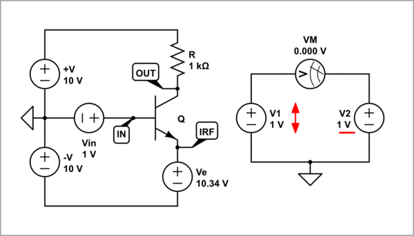
  • IRF - "immovable" ground

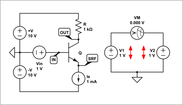
  • SRF - "self-movable" ground

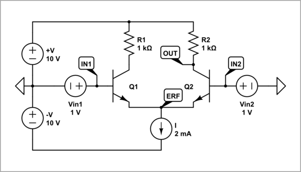
  • ERF - "externally movable" grounds

"Immovable" ground

Of course, to change a voltage, for example, across the voltmeter VM (in the figure below on the right), we must "fix" the voltage (V2) of one of its terminals and apply the input voltage (V1) to its other terminal... ie. we need an immovable ground.

schematic

simulate this circuit – Schematic created using CircuitLab

We can see this arrangement in a common emitter stage (the figure on the left) where the emitter voltage Ve is fixed by a constant voltage source and the input voltage Vin is applied to the base. As a result, the stage has a maximum voltage gain.

Notice that the emitter voltage source is connected to the negative power supply -V instead to ground but I have adjusted its voltage so that the difference across the base-emiter junction is about 0.7V. Change it gently (in millivolts) because the current changes abruptly.

"Self-movable" ground

But what happens when the reference voltage V2 does not stay constant but changes simultaneously and in the same way as the input voltage V1? The input voltage "does nothing"; the voltage difference across the voltmeter (V1 - V2) does not change.

schematic

We can observe this phenomenon in a common collector stage (emitter follower) where the transistor itself moves its emitter voltage (the reference point) so that it is (roughly) equal to the input voltage. As a result, the stage has a minimum (unity) voltage gain.

So the conclusion is that there is not internal ground in the emitter follower.

Notice that the current source in the emitter plays no role here because it is shunted by the transistor "voltage source" (the emitter follower).

"Externally movable" reference point

Ok, in a common emitter stage there is a "fixed" ground, in a common collector stage there is a "movable" ground... But what do we do when we need both?

Differential pair. Such a need appeared almost a century ago when they invented the famous long-tailed pair. Then there were already two input voltages that could change in different ways. When they changed simultaneously and in the same direction (common mode), the ground was supposed to be "mobile" to have no gain, and when they changed simultaneously and in the opposite direction (differential mode), the ground was supposed to be "immovable" to have gain.

They brilliantly solved this problem by connecting (through their outputs) two emitter followers. So they can interact to produce different types of ground.

schematic

simulate this circuit

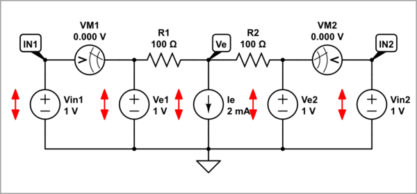
Equivalent circuit. I also made the equivalent electric circuit diagram just to follow the tradition but it turned out quite complicated. I put the two 100 ohm resistors because CircuitLab does not allow parallel connection of voltage sources. Maybe it is right because they are ideal and the resistors make them real. Anyway, this is another good inventive principle - "to do something upside down"... and to everyone's surprise, the result to be positive.

schematic

simulate this circuit

As you can see from the diagram, there are a total of five sources - four voltage and one current. The sources Ve1 and Ve2 are "clones" of the input sources Vin1 and Vin2. The schematic is conceptual and does not correspond exactly to the original one where only two voltage sources are really sources (producing power). Here they are all shown as true sources and therefore the directions of the currents do not match the original ones... but that does not really matter for understanding the idea.

In the middle of the circuit diagram, we see three sources - Ve1, Ve2 and Ie, in parallel. They are essential to our purpose... and especially the middle (reference) point with voltage Ve.

Exploring the differential pair

In common mode, the two emitter followers cooperate and together move the common "soft" ground. The two input voltages "do nothing"... the collector currents and accordingly, the output voltage Vout, do not change... there is no gain.

In differential mode, the two emitter followers oppose each other, each keeping the common ground stationary (trying to "move" it in the opposite direction) while the other tries to "move" it in its direction. The two input voltages have full control over the collector currents; they and accordingly, the output voltage Vout, vigorously change... there is high gain.

Conclusion

There is no permanently fixed ground at the midpoint between the emitters of the op amp's input differential stage because common mode requires it to follow the input voltages.

In differential mode, each of the input sources acts as a ground for the other.

The common mode removes the ground and differential mode creates it.

\$\endgroup\$
0
\$\begingroup\$

The DC output voltage will appear at your output based on your DC gain and input bias voltage. The op-amp will amplify anything as long as it's in its linear region of operation (i.e. all transistors remain in saturation and probably other requirements too).

The 1st 3 amplifiers on your first row end up at 0v simply because your input DC bias is 0V and the DC gain from input to output is 1V/V. If you see some minor deviations, is most likely due to the op-amp's own voltage offset. The change is relatively small.

The 2nd row has a DC gain of 2V/V, hence, any DC input voltage will appear at your output multiplied by 2.

You can also not reference the feedback network in your 2nd row to ground, but to any arbitrary voltage instead. When you do that, you'll keep having your same 2V/V non-inverting gain. However, this new voltage you have placed will have a DC gain of -1V/V to the output as well. You simply sum both of their outputs. This new voltage will be subtracting from non-inverting amplified 1V input voltage at the (+) input of the op-amp.

In both rows, as long as you're within your opamp's input common-mode range and output swing compliance (meaning, you're not too close to either +/-VDD), it'll amplify the DC signals as I mentioned previously.

You can grab that 2-stage amplifier schematic and place it instead of the op-amps you simulated before, same principle applies.

As you said, everything starts with the common-mode voltage and negative feedback. When you connect the output to the (-) input, you have one degree of freedom to define the output voltage you want to see, and that is set at the (+) input. The constraint is that this input voltage has to be such that all your transistor still remain in saturation, and this is usually a range of voltages. For instance, QP4 in the schematic is a current source. If the DC bias you apply at the (+) input is too high, the op-amp will try to minimize this DC difference by generating the same DC level at the (-), but it might drive QP4 out of saturation and into the linear region, thus, your op-amp isn't in its linear region anymore, it's useless.

Extra wrinkle:

Single-ended input stages are also used sometimes when very low-noise is required.

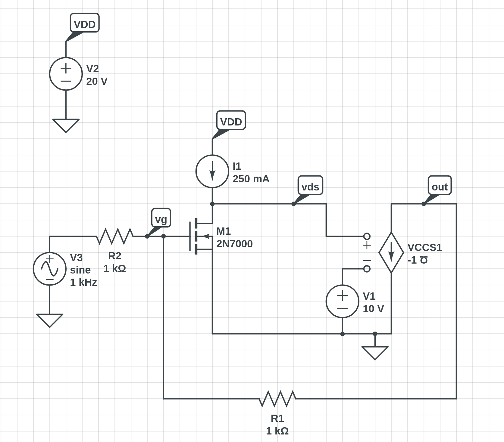
semi-ideal inverting feedback amplifier

If the input DC voltage is 0, and M1's VGS is 4V (obtained by simulation, and determined the loop), do you know what's the output voltage?

It'll be 8V.

Why? the VGS voltage sees a non-inverting amplification path towards the output. If we add another resistor parallel to R2, we can tune this output voltage such that we end up at half-supply at the output, while the M1's VGS remains at 4V. This flexibility can be very useful because decouples the biasing of the input and output stage, which can be biased for optimum noise and optimum distortion, respectively.

\$\endgroup\$

Your Answer

By clicking “Post Your Answer”, you agree to our terms of service and acknowledge you have read our privacy policy.

Not the answer you're looking for? Browse other questions tagged or ask your own question.