2
\$\begingroup\$

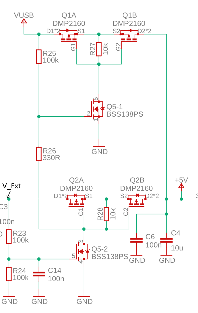
The schematics of the Arduino Uno WiFi Rev2 available here as PDF show the following topology used in the input voltage detection and protection circuitry, where regulated, external power supply comes from the left, and the USB Bus supply is coming in from the top:

Power supply circuit

What is the purpose of this circuit? How does the MOSFET topology work here? Does it offer additional protection against "back flow" if both USB and external power are connected?

I'm struggling hard with analyzing the MOSFET interaction here, especially the back-to-back n-channel MOSFETs at the top.

Thanks!

\$\endgroup\$
1

2 Answers 2

1
\$\begingroup\$

They're actually back-to-back P-channel MOSFETs. On the left, the Q1A pMOS is connected "backwards" in what is called an "ideal diode" configuration. As it's behaving like a diode, it blocks current flow if the power supply is connected in reverse.

Under normal operation, the body diode in the pMOS conducts from the drain to the source. There's an immediate voltage drop of around 1 V, but then provided the Q5-1 nMOS is conducting, R27 will pull G1 below S1, turning on the pMOS's conductive channel and reducing its resistance to a few tens of milliohms. Very little power is lost.

However, if voltage is connected backwards, the body diode in Q5-1 conducts, holding G1 and S1 at the same voltage, closing the Q1A conductive channel. S1 is also higher than D1, so the Q1A body diode blocks. No current can flow, and the circuit is isolated from the reverse voltage.

Q1B appears to do something similar to block a voltage connected at V_ext from being fed back up the USB line. If V_ext has a voltage connected, Q5-2 will conduct, pulling down the gate of Q5-1 via R26. If Q5-1 is off, Q1A and Q1B are both turned off. However, the body diode of Q1A will still conduct, so Q1B is needed to actually close the channel. Under USB-powered operation, Q1B is on at the same minimal resistance as Q1A, so again very little power is lost. Specifically, this configuration prioritizes V_ext: if there's power at V_ext, the USB power is cut off.

Q2A performs the same reverse-polarity function, but protecting V_ext instead. It also prevents power from 'back-feeding' up V_ext from the USB power line, as Q5-2 is off, holding Q2A's source and gate at the same voltage through R28. However, I'm not exactly clear what Q2B is doing here: when V_ext has voltage, it conducts; when only USB voltage is present, it conducts through its body diode.

Finally, bang in a couple of power filter capacitors and you've got your design as pictured above.

\$\endgroup\$
4
  • 1
    \$\begingroup\$ Thanks a lot! That explanation was very easy to follow. \$\endgroup\$
    – katharina
    Commented Feb 12, 2023 at 22:07
  • 1
    \$\begingroup\$ "However, if voltage is connected backwards, the body diode in Q5-1 conducts" could you explain why this happens? Do you mean VUSB being wrongly connected, or VExt? How does this cause the body diode to conduct? \$\endgroup\$
    – katharina
    Commented Feb 12, 2023 at 22:16
  • 1
    \$\begingroup\$ @katharina Specifically for Q5-1, USB voltage must be backwards -- i.e. ground must be at a higher potential than VUSB. No diode is "perfect", so even though this circuit shows two diodes with cathodes connected, some small leakage current will flow through both. If Q5-1's drain is already at 0 V, it will quickly rise to 5 V through the body diode; this will pull the node at Q1A G1 to 5 V directly, and then after some small (nanosecond-scale) time period, also pull Q1A S1 to 5V through R27. Now, Q1A D1 is at 0 V and Q1A S1 is at 5 V, so the Q1A body diode is only letting picoamps through. \$\endgroup\$
    – Matt S
    Commented Feb 12, 2023 at 22:23
  • 1
    \$\begingroup\$ If, on the other hand, VUSB is floating and Vext is backwards, the current through R25 and R26 will still pull VUSB to a nominal 5 V, but since nothing's connected to it, nothing will happen. And Vext will be blocked by the 5V appearing at Q2A S and G. In both cases there are resistive paths connecting GND to the voltage outputs, so some small current will still flow in a reverse connection, but through 100K resistors, so it's just a few dozen microamps and it's not going anywhere near any sensitive silicon. \$\endgroup\$
    – Matt S
    Commented Feb 12, 2023 at 22:24
1
\$\begingroup\$

Notice first that there are two identical structures repeated, consisting each of two PMOS, a 10k resistor, and NMOS arranged in a sort of T shape. A positive voltage on the gate of the NMOS allows current through, pulling the two PMOS gates down and effectively opening a path through their drains. This is a voltage controlled switch implemented with MOSFETs.

Imagine for a second that the bottom of R26 is unconnected. In this modified circuit, the presence of VUSB places the full 5 volts on the NMOS gate, opening the switch and allowing VUSB to power +5V.

If you ground that same end of R26, the NMOS gate voltage will drop almost to zero due to R26 being much smaller than R25, thus cutting off VUSB from +5V. This means you can use a low voltage at this point to "supersede" the 5 volts available from VUSB, which the full circuit indeed does.

V_Ext is connected to an identical gate circuit, whose NMOS also pulls this "supersede" signal from the previous structure low. The full circuit thus gives priority to V_Ext. If Both V_Ext and VUSB are present, V_Ext is connected to +5V. If only VUSB is present and V_Ext is open, then Q5-2 will have zero volts at its gate, and R26 will be seeing an open circuit, opening the VUSB "switch", allowing VUSB to power +5V.

Edit: This circuit does actually provide backflow prevention between +5V and VUSB, now that I simulate it.

\$\endgroup\$

Your Answer

By clicking “Post Your Answer”, you agree to our terms of service and acknowledge you have read our privacy policy.

Not the answer you're looking for? Browse other questions tagged or ask your own question.