1
\$\begingroup\$

Problem

I have designed an active low-pass filter using Sallen-Key architecture. It is a 4th order filter (two 2nd order stages cascaded). Here is the circuit diagram:
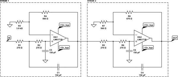
schematic

simulate this circuit – Schematic created using CircuitLab

+-12v_byp are +- 12V power supplies bypassed by 2.2uF and 0.33uF tantalum capacitors.

LM6171B (datasheet) has GBW of 100MHz. I arrived at the component values using a combination of equations, such as $$F_c=4\text{ MHz (goal)}=\frac{1}{2\pi RC}$$ for the simplification where resistor and capacitor values are equivalent.

LTSpice frequency analysis

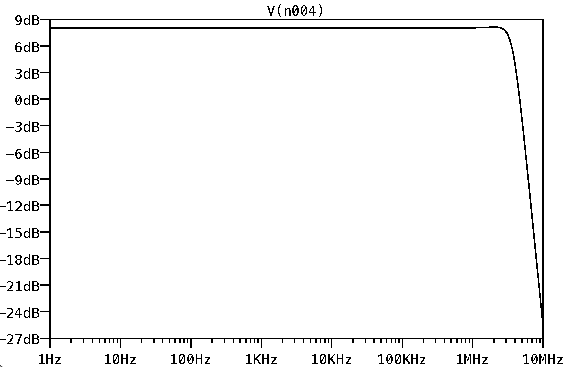
LTSpice AC analysis is nominal and has a cutoff at 4 MHz:

enter image description here

Real-life result

I built the circuit on a solderless breadboard, taking care to choose capacitance values large enough to render parasitic capacitances negligible. Still, the experimental behaviour of the filter deviates from the simulation:

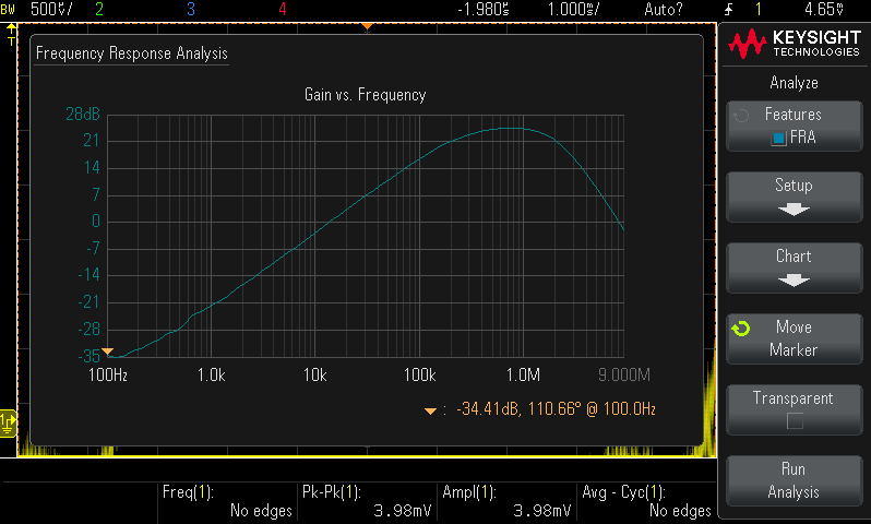
Scope shot (Frequency response analysis)

The filter behaves more like band-pass than low-pass and strongly attenuates very low frequencies below 50kHz.

What are some possible reasons for this behaviour? The only thing I can think of are parasitic capacitances on the breadboard, but I have tried to take these into account through component choices. Also, shouldn't these parasitic capacitances affect high-frequency signals more than low-frequency ones?

\$\endgroup\$
13
  • \$\begingroup\$ Why are you showing the wrong LTspice analysis graph? Why is the gain so badly wrong? I expect that your breadboard implementation may be wrong also. It's miles off the 8 dB gain you appear to be wanting. \$\endgroup\$
    – Andy aka
    Commented Feb 14, 2023 at 15:29
  • \$\begingroup\$ Looks like a band pass filter response. Also, what does this mean, "taking care to choose capacitance values large enough to render parasitic capacitances negligible"? You need to use the values from your design in order to get the designed behavior. \$\endgroup\$
    – Aaron
    Commented Feb 14, 2023 at 15:29
  • \$\begingroup\$ Hi @Aaron—when designing the filter, larger capacitance values were chosen a priori and resistance values followed. That's what I meant. The component values are theoretically sound and match the design exactly. \$\endgroup\$
    – javan.g
    Commented Feb 14, 2023 at 15:31
  • \$\begingroup\$ @Andyaka, I believe the LTSpice absolute gain is wrong due to the DC bias being set to 0 in the simulation? I understood this was less important when considering pure ac response. As for the breadboard circuit, I've quadruple checked this with peers and professionals and they agree the implementation is as drafted. \$\endgroup\$
    – javan.g
    Commented Feb 14, 2023 at 15:33
  • \$\begingroup\$ Another thing to check is that the scope plot starts at 100Hz whereas the LTSpice plot starts at 1MHz. From 1MHz to 9MHz they are similar....not the same, but both low pass. What does LTSpice show when starting at 100Hz? \$\endgroup\$
    – Aaron
    Commented Feb 14, 2023 at 15:34

2 Answers 2

1
\$\begingroup\$

I started out just doing a few quick calcs. In your first stage I find that \$\zeta_{_1}=2-\frac{560\:\Omega}{3.9\:\text{k}\Omega}=1.85641\$ and therefore that \$A_{v_1}=3-1.85641=1.14359\$ and for the second stage that \$\zeta_{_2}=2-\frac{670\:\Omega}{560\:\Omega}=0.80357\$ and therefore that \$A_{v_2}=3-0.80357=2.19643\$. Combined, I'd expect a total 2-stage gain of \$A_v=1.14359\cdot 2.19643=2.5118\$ and therefore \$20\cdot\log_{10}\left(2.5118\right)=8\:\text{dB}\$. (Actually 7.9997 dB.)

With that in hand I just popped in two opamps with 80 MHz gain-bandwidth that I use a lot for "just simulating": the LT1800:

enter image description here

Looks fine to me in simulation. The gain is exactly what I expected to see in the passband and the -3.01 dB point is about where you figured, too. (Click on the image to get a larger view.)

Your simulation was wrong. But it is nice to hear that when you used "1" for the AC input source that you did get the right results.

It is very difficult to use a solderless breadboard in this case. There is way, way too much stray capacitance (in the breadboard itself) and inductance (in the wiring) for something like that.

For comparison, even if you are still required to later use a solderless breadboard, first give it a try using manhattan style construction (or dead-bug) and see where that gets you. If that removes the problem and its successful, you now have a benchmark to work against by comparison when working to reproduce results on the solderless breadboard. If on the other hand, that does not remove the problem, then you've got some other issue to contend with.

\$\endgroup\$
3
  • \$\begingroup\$ " it is very difficult to use a solderless breadboard here." Yes. Yes. Yes. Not only due to the mentioned issues, but also the more basic unreliable connections. Trust nothing on a breadboard. Dead bug it. \$\endgroup\$ Commented Feb 14, 2023 at 21:26
  • \$\begingroup\$ Thank you for your help. I've identified the problem in my simulation—it was just that the AC amplitude was not set to 1. Setting it to 1 fixes the simulation issue. As for solderless breadboards, I agree that it is non ideal but I don't have much choice here (this is a class project and this is the medium required). This specific kind of circuit has also been built in this class previously and seemed to function fine with the same frequency parameters. \$\endgroup\$
    – javan.g
    Commented Feb 14, 2023 at 22:11
  • \$\begingroup\$ @javan.g Then you will require a great deal of care and awareness of the issues. Clearly, others are telling you it is fine and you are failing to get it done right. Now that the simulation shows the right things, you've only your construction methods left to blame. \$\endgroup\$ Commented Feb 14, 2023 at 22:33
0
\$\begingroup\$

C1 and C4 provide positive feedback for high frequencies. While that can be useful for narrowing the transition region, they seem large in comparison to other components.

Then there is "+-12v_byp are +- 12V power supplies bypassed by 2.2uF and 0.33uF tantalum capacitors.". Some people translate "bypassed" into "poisoning the reference ground" Bypassing should happen to a ground power rail, not to the signal ground track. The point of the bypass ground is to source and sink current spikes better than the power rails, and the signal ground is definitely the wrong place for sourcing and sinking current spikes.

But that's more of a side note not likely related to the completely different behavior you see.

The main difference I consider likely between your simulation and reality (assuming that you properly implemented all of the circuit) is that the voltage source in your simulation has an impedance of 0ohms while your real input has a non-zero impedance.

In particular because of the positive high-frequency feedback of C1, any non-zero impedance of your signal source will lead to an inflated high frequency response (if not downright oscillation) compared to the simulation.

You might want to add a buffering opamp to the input stage in order to remove the input impedance effect on your frequency response.

\$\endgroup\$

Your Answer

By clicking “Post Your Answer”, you agree to our terms of service and acknowledge you have read our privacy policy.

Not the answer you're looking for? Browse other questions tagged or ask your own question.