What is the difference between "Solder mask expansion" and "Solder mask to copper clearance" in KiCad-7 PCB design software?
1 Answer
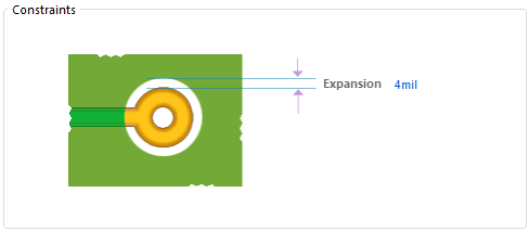
Solder mask expansion: This parameter defines the amount by which the solder mask layer extends beyond the edges of the copper pads or traces. A positive value means that the solder mask will cover a larger area than the copper, while a negative value means that the solder mask will be smaller than the copper. The purpose of the solder mask expansion is to ensure that there is enough solder mask material between adjacent copper features to prevent shorts and other assembly problems.
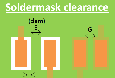
Solder mask to copper clearance: This parameter defines the minimum distance between the edge of a copper pad or trace and the edge of the solder mask that surrounds it. The purpose of the solder mask to copper clearance is to ensure that there is enough space for the solder to flow and form a strong bond between the copper and the component during the assembly process. If the clearance is too small, the solder may not flow properly, leading to weak or unreliable connections.
-
\$\begingroup\$ Can this question and answer be updated to include solder mask minimum web width for completeness? Also, in your image, can you specify which is the soldermask to copper clearance — E or G (Does solder mask mask to copper clearance include the solder mask expansion?) \$\endgroup\$– kandoCommented Mar 17, 2023 at 19:36


