1
\$\begingroup\$

UPDATE AT THE BOTTOM

in a battery powered project with high current I'm using a P MOSFET as load switch in place of a mechanical switch to prevent inrush current and consequent spark on the switch contacts. The battery is rated 36V (as being Li-ion let's consider 42V at full charge) and 15A at max discharge.

The SPDT switch that originally was on the positive rail of the battery (this way sparking when turned on) now is located on the gate of the P MOSFET.

What accidentally happened is that, being the first time using and experimenting with discrete MOSFETS, I measured Vgs in strict reference to GND.

This is clearly a mistake: to turn the MOSFET off, I placed a resistor of 1.2M between source and gate to obtain something under 20V (measured towards GND) to stay under the absolute max rating for this MOSFET; to turn it on, the GATE is directly routed to GND by the SPDT switch. the first configuration
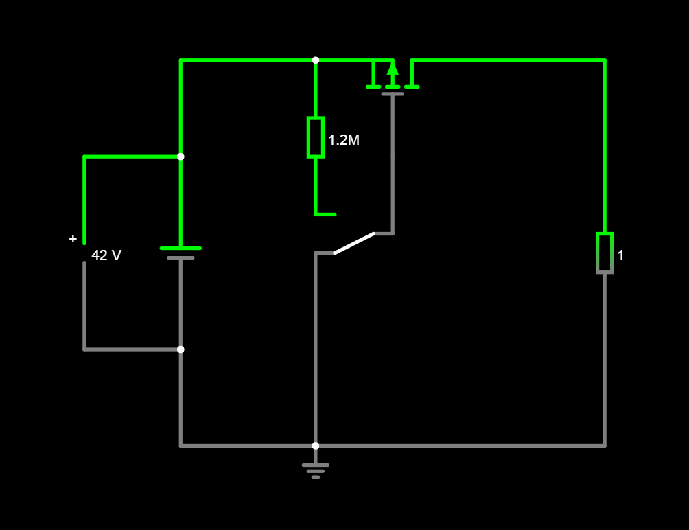
Still before realizing that, in reference to source, Vgs is something near 22V when off and 42V when on and then always beyond the absolute max ratings, I obtained a fully working circuit and further I get my resulty with no damage to the MOS.

Now I know that the correct circuit would be instead this: the correct circuit
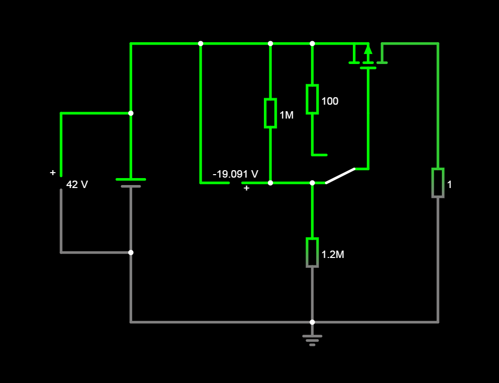
where the resistor to source is just a current limiter but Vgs must reach virtually 0V; the resistor to ground must be measured in order to obtain something near -20V for Vgs and it obviously needs a pull up resistor to make a divider.

Assuming that's common that with newest generation Power MOSFETS Vgs can exceed until 80V without damage, I can't still figure out why the circuit is working both on and off also if Vgs is always far beyond any expected rating.

The MOSFET never gets warm, because being an on/off main switch is not used often, but some days are passed in off state and I assume Vgs is always near 40V (and it's still working fine!)

I would notice that in early experimentation I was using an old, discontinued Power MOSFET with something near 0,1 Ohm as Rds and the device was dissipating near 26W, with a minor reduction of battery lasting with the same load. For this reason I changed to a newest Power MOSFET with the minimum Rds available to reduce the loss.

What do you think about this strange behaviour?

Being thankful to You in advance, I give my best regards

Fabio

UPDATE: Hello again.

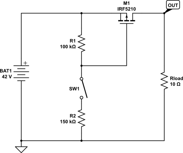
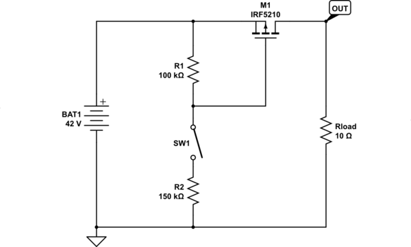
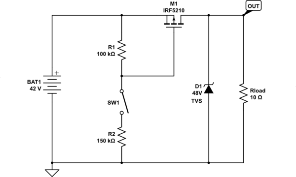
I tried to build the circuit suggested by Simon, having a Goford Power P-MOSFET with the source connected to the positive supply of the battery (+42V), the drain to the load, a 100k resistor between source and gate to provide 15Vgs, the switch that shorts this gate configuration to another 150k resistor ending to the negative supply of the battery (0V) AKA the whole ground load.

the actual MOSFET configuration suggested by Simon

Only one board worked, some months ago, so I sold the product. It's very far from me, but it's working good. So I produced 30 boards with this exact circuit for the MOSFET implementation. But also if nothing has been changed in the board design, any other attempt on new boards is producing a fail on the MOSFET. I can say this because something like 9 MOSFETS has gone into failure in a board that's exactly the same revision of the working one.

Actually 11 MOSFETs of 12 are gone. The last Goford was placed on a brand new board with brand new components. It's important to say that everything on the load side is working perfectly. I tried with a IRFP9140N too to exclude the consideration of a defective batch. No luck. The majority of the MOSFETs went short at the first power up with no external signs, some lasted just a bit. Basically we have short on source-drain junction, or also the gate with source and drain. The failure seems due to Avalanche effect.

The load board, that works perfectly as expected, provide the parallel supply of two audio power amplifiers (automotive class D and class AB ICs) with power exceeding 350WRMS plus three voltage regulators (one LM317 and two LM338) for auxiliary supply; the board has been designed with a full ground plane and has been cared as requested from the class-D data sheet: as you know, class-D amplifiers must be routed with great care to work properly. Of course, there are capacitors for more than 13500uF as reservoir.

One of the three regulators supplies a secondary board with preamp section and MCU, but for sure this is not the issue, as the MOSFETs fail also with this secondary board disconnected.

I'm suspecting the MOSFET must be protected with a 42V zener diode or a snubber network between drain and source, but I wait for your precious opinions.

It's also important to say that a product unit I have with me adopts the original configuration with just a 1.2M resistor from source and the switch hanging around between this resistor and ground, IRFP9140N P MOS. It still works good with no stress signs.

Thank you very much

Fabio

UPDATE AGAIN: Here came the brand new Infineon automotive high side switches in TO-220 sipmos package, with a rating so much higher than I need. These fails exactly the same way, at the first connection of the battery the MOSFET inside becomes shorted.

Apparently a 100nF capacitor between source and gate, as Tobalt suggested, solved the problem on my last IRFP9140N. Still have not tried the same solution on the smart high side switches, expecting that a specifically designed device for inrush currents would take this into account. Probably it gets the same: next boards will say.

Having made a lot of trials when I packed the only working system I sold, I suspect I adopted the capacitor and I forgot it between the processes as I forgot to add it to the last PCB revision, because seems there's no other possibility to get the thing to work properly without this one. As I can't check neither open this only working piece, honestly I was lacking for considerations.

Thank you all, especially to Tobalt, Simon Fitch and Greybeard.

\$\endgroup\$
12
  • \$\begingroup\$ With more than 10 mF "reservoir capacitors", you may need a way to limit rush-in current. With a 1.2 M gate resistor to 40 V, turn on will be slower than 60 k to 16 V. (Why use a P-channel transistor?) \$\endgroup\$
    – greybeard
    Commented May 16, 2023 at 7:48
  • \$\begingroup\$ hello greybeard, the inrush current is exactly the problem that brings to use the MOSFET. Originally the system was powered up directly with a SPDT switch: at any power-up the switch sparked, stucking a lot of switches just after the first time. So the next steps brang the MOSFET solution to use the SPDT as Vgs control instead of direct current switching. \$\endgroup\$
    – Fabio
    Commented May 16, 2023 at 7:52
  • \$\begingroup\$ @greybeard I'm using the P MOSFET because anything on the load (PSU board + preamp board) must be directly connected to GND. It's also the simplest way to connect the battery, I tried a N MOSFET too but requires more work... and has yet blew a pair of N MOS. I went for P MOS and I was pretty happy, but now these are failing. \$\endgroup\$
    – Fabio
    Commented May 16, 2023 at 8:02
  • \$\begingroup\$ There are "automotive high-side switches". \$\endgroup\$
    – greybeard
    Commented May 16, 2023 at 8:05
  • \$\begingroup\$ Thanks @greybeard. Do you think there's no way to avoid to change the whole design again? Preventing the Goford MOSFET to fail because of this inrush current would be the preferred solution. \$\endgroup\$
    – Fabio
    Commented May 16, 2023 at 8:17

3 Answers 3

2
\$\begingroup\$

Exceeding max Vgs may not blow the MOSFET right now if you're lucky, but it's certainly not safe.

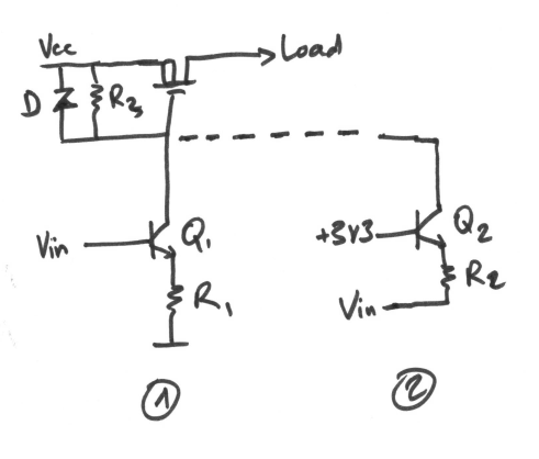
Here are two circuits:

enter image description here

Assuming it is driven by a microcontroller with a known high level output voltage, for example 3V3.

#1 uses transistor Q1 and resistor R1 to make a current source. For example with Vin=3.3V, we have 2.7V on R1, so with 2.7kOhm it will make a 1mA current source. This goes through Q1 and creates a Vgs on the MOSFET, which is limited by zener diode D (for example 15V). Resistor R3 serves as pullup to turn off the MOSFET. If we use 15kOhm for R3, then with the 1mA current through Q1, Vgs will be limited to 15V anyway so the Zener diode can be omitted.

#2 puts the input on the end of the resistor, and Q2 base is set to 3.3V. It does the same, but inverts the logic, so it will turn on the MOSFET if Vin=0V.

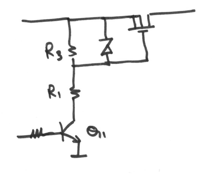
Another one:

enter image description here

In this case R1 will have to be higher value to drop the higher voltage difference. The drawback is you need an extra resistor for Q1 base, and if the power supply isn't high enough the MOSFET can potentially receive a low Vgs which turns it on partially instead of fully. So you get an unexpected failure mode where the FET smokes because supply voltage is too low. The two previous versions will turn on the MOSFET fully as long as the supply voltage exceeds 3V3 + required Vgs, and they're much more flexible wrt supply voltage.

\$\endgroup\$
1
  • \$\begingroup\$ the idea is to keep the switching circuit as simplest as possible still using the main physical switch, so no MCU or level shifting BJT operation, this because... the load side is exceptionally complex to build!!! :) and as long as I have to build a lot of units, I don't want to complicate things further. I know what you say about safety: the first circuit is still alive, still works perfectly despite the strange phenomenon, but clearly I prefer to solve it with previdence for a future unexpected fault. \$\endgroup\$
    – Fabio
    Commented Mar 11, 2023 at 18:56
2
\$\begingroup\$

As you have it, the gate is able to spend some time completely disconnected, as the switch moves from one position to the other. This is not advisable, since the gate can vary wildy in potential while floating like that. I'm sure you can imagine what effect this might have on whatever load you connect to the output.

The solution is to make sure that the gate always has a current path to somewhere, with a resistance.

You require is that the gate-to-source voltage \$V_{GS}\$ be either zero, or some fraction of the total supply voltage, but never floating. That's easy to achieve with just two resistors and an SPST switch:

schematic

simulate this circuit – Schematic created using CircuitLab

You don't even need a double-pole switch. With SW1 open, the MOSFET gate discharges to \$V_{GS}=0V\$ via R1.

When SW1 is closed, R1 and R2 form the potential divider which applies a fraction of BAT1's voltage the gate. That fraction is \$\frac{R_1}{R_1+R_2}\$. Using the values shown, that's 40%, for \$V_{GS} = 40\% \times 42 = 17V\$.


Update

There are a few immediately obvious candidate problems:

  1. The supply momentarily exceeds the FET's max \$V_{DS}\$. It would be unusual for this to arise on the battery side,, so presumably this is caused by the load (an inductive one, for example), or some other voltage source. Are you switching to battery when another source goes away?

  2. \$V_{GS}\$ is still somehow exceeding its maximum, which would probably be related to (1).

  3. Switch bounce is causing the gate to rise and fall, causing the transistor to transition between on/off states, with the associated power dissipation.

  4. Gate potential is not rising/falling fast enough, causing the FET to linger too long in a state between fully on or off, where it dissipates excessive power.

To protect the MOSFET from supply spikes, try a using a TVS diode:

schematic

simulate this circuit

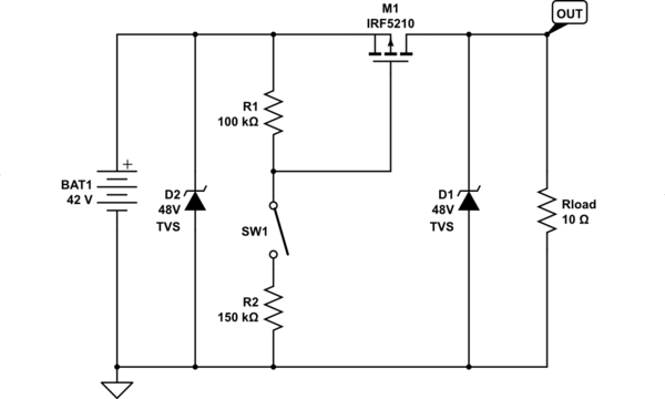
As long as the killer condition is short lived, and infrequent, D1 should clamp voltage. While I don't think the battery is the source of your problems (unless you have long supply wiring in a big loop), you could install a TVS diode on the battery side too:

schematic

simulate this circuit

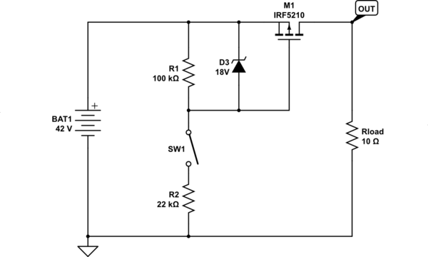
Prevention of excessive \$V_{GS}\$ is easier, using a regular zener diode, D3 below. I've also reduced R2, since \$V_{GS}=18V\$ is ensured by the diode, and we no longer rely on the resistor divider for that. The diode simultaneously prevents \$V_{GS}\$ becoming more negative than -0.7V, also a potential hazard:

schematic

simulate this circuit

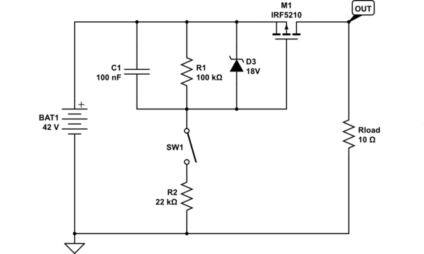
Switch bounce is always a problem, and the best solutions would employ a schmitt trigger of some kind, but for simplicity you could mitigate the issue with a capacitor, C1 below. When the switch is closed, the capacitor takes a millisecond or so to charge to 18V via R2, but when the switch is opened it discharges much slower, via R1. This prevents gate potential from flapping wildly up and down as the switch bounces open and closed. It does slow the switch-on and -off times of the MOSFET somewhat, don't be afraid to use a smaller capacitance; say 10nF, to improve switching time, at the expense of debouncing efficacy:

schematic

simulate this circuit

High values of R1 and R2, combined with gate capacitance, already produce a somewhat slow slewing gate potential, and that's exacerbated by adding switch debouncing capacitance C1. To mitigate this, it's probably necessary to drive the gate from a lower impedance source, with gain, requiring an additional transistor:

schematic

simulate this circuit

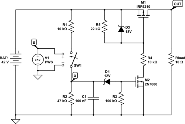
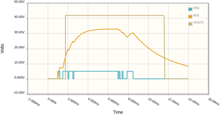
It's a lot, I know, but this will switch on and off M1 much more emphatically, while simultaneously debouncing SW1. Ignore V1, it's for simulation only. M2 replaces the original SW1, and gives us voltage gain. D4 raises the switching threshold of M2 somewhere near +15V, so the potential at X must rise and fall through +15V to switch on/off M2. X rises and falls quite slowly, due to debouncing capacitor C1. Resistors R5 and R4 can be much lower impedance than the previous gate periphery, increasing M1's gate current and improving M1's switching time.

In my simulation, blue is switch state, where you can see simulated bounces. You see how this affects \$V_X\$ (orange), which rises and falls quite slowly, but M1 is switched on and off much more sharply, as you can see at OUT (brown):

enter image description here

There must be a dozen different ways to do this, and I don't claim this is the best or simplest, it's just an example. Also, I didn't test this except in the simulator, to verify that it works in principle and nothing's dissipating excessive power. If you build it, be sure to test the thing thoroughly prior to deployment.


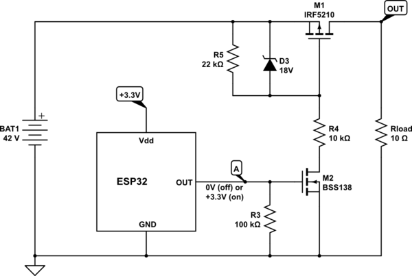
The use of M2 permits you to control M1 with a digital signal, instead of a switch:

schematic

simulate this circuit

A high digital signal (+3.3V or +5V, for instance) at A will switch on M1. No debouncing necessary. Perhaps you can build a module with both options in mind, physical switch or digital signal.

\$\endgroup\$
12
  • \$\begingroup\$ Hello Simon, thank you very much for this suggestion. I have only a question: do I will reach Vgs=0V with a current limiting resistor of 100k? To drive the gate I tried yet some values (100k too) and a measurable (referred to GND) voltage drop always occurred. I'm just wondering that such high value could leave some current circulating in the system when turned off, this way slowly discharging the battery pack. But yes, leaving the gate always connected is the best thing. Thank you \$\endgroup\$
    – Fabio
    Commented Mar 12, 2023 at 20:17
  • \$\begingroup\$ @Fabio No resistor in these circuits are to be considered as limiting current. On the contrary, they all provide a path for current to flow. In the case of R1, yes, it will cause \$V_{GS}=0V\$ when SW1 is open, and it is the only way the gate capacitance can discharge. 100kΩ will do that just fine, if a little slow. Your own value of 1.2MΩ does it even slower. Since the gate has almost infinite resistance to anything else, no current will flow from the battery via R1 (or R2) while SW1 is open. \$\endgroup\$ Commented Mar 13, 2023 at 3:32
  • \$\begingroup\$ @Fabio In your second circuit, there's a permanent path from +42V to ground via the 1M and 1.2MΩ resistors. That path will always draw current from the battery, regardless of the switch position, or state of the MOSFET. \$\endgroup\$ Commented Mar 13, 2023 at 3:36
  • \$\begingroup\$ Good morning and thank you Simon for your clarifications. Today I will apply these, reporting the result with measurements. As yet said, MOSFETs (and discrete electronics in general) are new matter to me, but a new field to learn and it's worth it. \$\endgroup\$
    – Fabio
    Commented Mar 13, 2023 at 7:18
  • \$\begingroup\$ Hello @Simon Fitch, I want to update about the results after taking the due time. Yesterday many Goford mosfets blew with this exact setup. I carefully checked the circuit made in the cleanest possible way: source to the battery, drain to the load, 100k resistance between source and gate, gate connected to the switch, at the other terminal of the switch 150k resistance connected to the battery negative. The junction between source and drain shorts when first turned on, some survive a few turns on, but the longevity of this system is not reliable over time. \$\endgroup\$
    – Fabio
    Commented May 14, 2023 at 8:09
1
\$\begingroup\$

Normal MOSFETs will be damaged in no time if you apply U_gs = 40V, you would have between source and gate a low resistance.

Possibly 1: Because of the voltage drvider with the 1.2Mega Ohm and the surface-resistance (because of the "dirty" surface) to GND, the voltage could drop to 20 Volt.

Possibly 2: There are MOSFETs who have a z-diode integrated between the gate and source. Because of the 1.2MOhm resistor no damage could be done.

\$\endgroup\$
4
  • \$\begingroup\$ very interesting. When saying "dirty surface", you mean the mechanical contact is behaving like a steady resistance? With the actual configuration, the voltage divider consisting in the pullup resistor of 1.2Mohms theorically sets something like a (not present) 1M resistance to GND to reach a Vgs of 18.3V (referenced to GND), in off state. The discontinued MOS was a IRFP9140N, actually I'm using a more efficient GOFORD G080P06T and there's no mention to zener diodes for both the two, as long the manufacturers didn't mentioned its presence in the official datasheets. \$\endgroup\$
    – Fabio
    Commented Mar 11, 2023 at 18:56
  • \$\begingroup\$ By the way, the circuit works the same: it switches off the load at Vgs>20V, turning on with Vgs directly connected to GND. \$\endgroup\$
    – Fabio
    Commented Mar 11, 2023 at 18:56
  • \$\begingroup\$ If this works, with direct connection to GND and a voltage of ~40V, then you must have a MOSFET with a very good insulated gate. The gate always withstands a slightly higher voltage than specified in the data sheet. In any case, it is very unusual and you should not expect that such a gate can generally withstand so much more voltage than is guaranteed in the data sheet. There is always a certain scattering in the production of the silicon wafers, perhaps the mask for the exposure was shifted a bit so that the substrate is thicker at the gate. \$\endgroup\$
    – MikroPower
    Commented Mar 11, 2023 at 23:46
  • \$\begingroup\$ @Fabio I think you are confused by saying you connect Vgs to GND, and you seem to be measuring the gate voltage to GND. You need to measure between gate and source \$\endgroup\$
    – PStechPaul
    Commented Mar 12, 2023 at 1:31

Your Answer

By clicking “Post Your Answer”, you agree to our terms of service and acknowledge you have read our privacy policy.

Not the answer you're looking for? Browse other questions tagged or ask your own question.