3
\$\begingroup\$

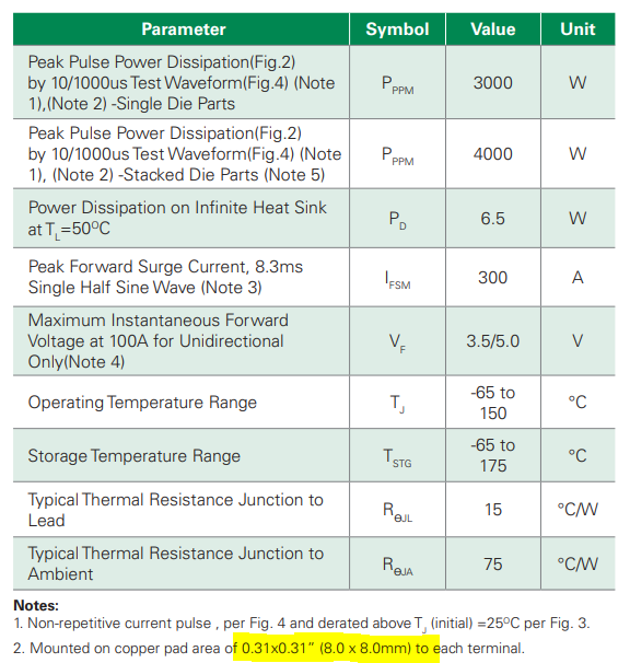
I am trying to understand how much power a SMDJ58CA TVS can handle during a very short moment (~ 20 µs.)

The information into the datasheet are the following:

enter image description here

enter image description here

enter image description here

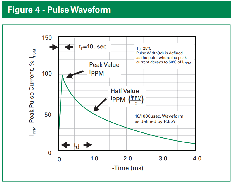
The peak pulse power rating @ 25°C for a waveform 10µs/1000 and the defined waveform:

enter image description here

enter image description here

enter image description here

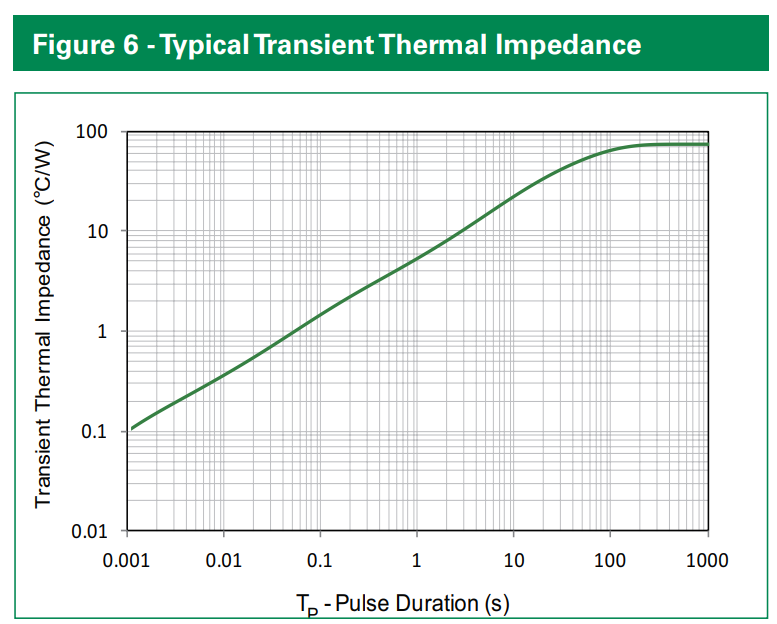
Suppose the footprint of the TVS corresponds to the datasheet (8x8mm on each pad.) My first idea was to used the average power over the time the TVS is dissipating power. Suppose the TVS has to dissipate a pulse power which looks like a square of power. Then I just have to multiply this power by the thermal impedance and get the junction temperature. If the junction temperature is higher than 150 °C, the TVS is undersized.

For 10 us, the thermal impendance is not given, the thermal impedance graph stops at 1ms. By interpolating, I could approximate it to 0.01 °C/W for 10 us.

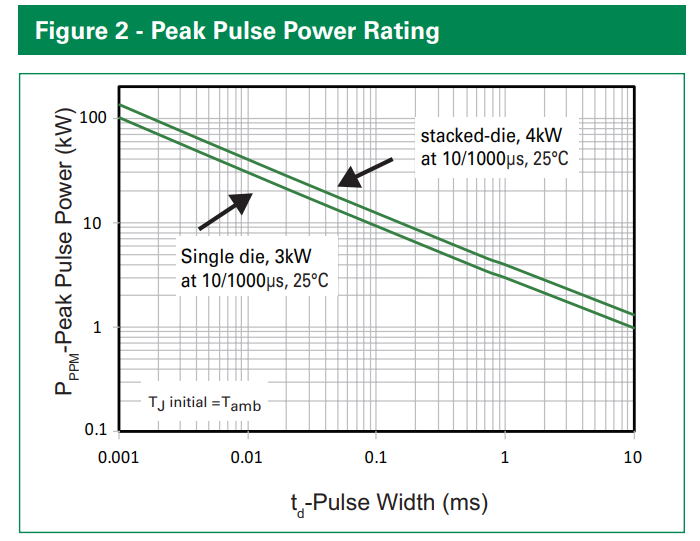
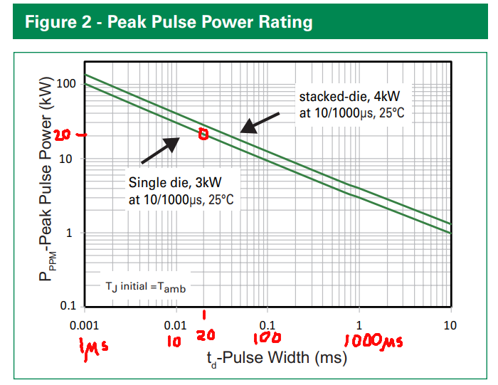
If we take a look @ Figure 2, "Peak power pulse rating", it is possible to evaluate the peak power power pulse for 10us and it seems possible to have a peak of power equal to 30 kW with the waveform 10us/1000, but when I take a look at the maximum clamping voltage @ Ipp(10/1000us) and the maximum peak pulsse current Ipp(10/1000us) the peak power pulse is only equal to 3 kW (93,6*32,1) and the waveform (10/1000us) is particularly different from my square pulse.

How is it possible to find the maximum peak pulse power of the TVS? Do you think that it would be possible to dissipate a square of 100 kW * 20us over the SMDJ58CA?

\$\endgroup\$
4
  • 1
    \$\begingroup\$ I think, grossly excessive surges would tend to result in bond wire vaporization (and subsequent explosion.) Medium-excessive surges may result in (spot) overtemp failures, with subsequent shorting and/or explosion. Slightly excessive surges seem to result in mostly just shorting. Only the datasheet numbers are guaranteed. Easy to simulate, calculate, test and measure with a charged cap; be careful. \$\endgroup\$
    – rdtsc
    Commented Apr 18, 2023 at 13:30
  • \$\begingroup\$ I think one can safely extrapolate the slope of the thermal impedance towards faster times because it is obviously dominated by the crystal heat capacity there. \$\endgroup\$
    – fraxinus
    Commented Apr 18, 2023 at 13:31
  • \$\begingroup\$ @rdtsc 100kW * 20us are 2 joules only so no enough energy for a fancy, military-grade explosion. \$\endgroup\$
    – fraxinus
    Commented Apr 18, 2023 at 13:33
  • \$\begingroup\$ @rdtsc FYI, these parts are made with lead frames, not wire bonds, AFAIK. So they have actually pretty good continuous power ratings (with lead or even body heatsinking). \$\endgroup\$ Commented Apr 18, 2023 at 17:19

1 Answer 1

1
\$\begingroup\$

The answer is in the question:

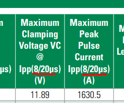
8/20us pulse rating

120.93 * 160.5 = 19... call it 20kW. This corresponds to the point in Fig.2,

Fig.2 highlighted at 20µs

Notice the 1/sqrt(t) scaling law, i.e. power rises one decade as time decreases every two decades. This is typical of a diffusion effect, i.e. heat is diffusing into the silicon die so the energy and power follow a diffusion (sqrt(t) or 1/) relation. This is further supported by the transient thermal impedance, which rises in a similar asymptotic manner; although not at the same slope as it turns out. Perhaps the slope changes in the >1ms time scale: this is where heat begins to spread out into the lead frame, at first the solder die attach and lead faces; then into the encapsulation and lead lengths, then after some seconds, finally into the PCB.

The time scale corresponds to distance traveled by heat. The relationship is the thermal diffusivity, which is roughly to say linear distance increases by √t. For silicon and copper, this rate is high, but for plastics, PCB, etc., it is quite low: hence it takes some seconds for heat to spread out into the board, and component heatsinking is completely irrelevant for pulses under some milliseconds. (It is relevant for repetitive operation of course, in terms of allowable duty cycle!)

Fig.2 is still for the peaky waveform, scaled by time; it is not a square pulse. As it happens, the peak power for such a waveform is about twice an equivalent square wave. Think of cutting off half the peak, and twisting it around to fill in the falling slope: now you have a square wave of half height and double width.

Likely more importantly: can you really allow such a high voltage drop for the connection? 160V from a nominal 58V or below is pretty dramatic, and indeed makes MOVs competitive -- TVS are best at low currents and low voltages, and this may be an application where MOVs excel indeed in all circuit parameters (energy and peak voltage); the one downside being, unless it is extremely large, the MOV will have a limited lifetime in such service (say thousands of events, depending on size).

As for 100kW at 20µs, clearly not. A 30kW (1ms) device will likely withstand that, however.

\$\endgroup\$
3
  • \$\begingroup\$ Thank you for your nice answer with a lot of useful information :) I have some questions. If we extrapolate the thermal impedance to 10 us, we can think that the thermal impedance is 0,01. And so 0,01*100kW = 100° which is ok at room temperature? I agree on what you said, but why the thermal impedance extrapolation is not correct ? \$\endgroup\$
    – Jess
    Commented Apr 18, 2023 at 16:18
  • 1
    \$\begingroup\$ The thermal impedance curve does not extend to lower time scales, so extrapolating it is of dubious value. Fortunately the peak power curve does extend down there, and indicates 1µs is acceptable at 100kW, and 20 most certainly is not. Why do you need so much power into such a small device, anyway? \$\endgroup\$ Commented Apr 18, 2023 at 17:21
  • 1
    \$\begingroup\$ I gave a possible explanation for the different slope. "...although not at the same slope as it turns out. Perhaps the slope changes in the >1ms time scale: this is where heat begins to spread out into the lead frame, at first the solder die attach and lead faces; then into the encapsulation and lead lengths, then after some seconds, finally into the PCB." These parts use a flat-metal lead frame, not wire bonding, AFAIK. \$\endgroup\$ Commented Apr 18, 2023 at 17:23

Your Answer

By clicking “Post Your Answer”, you agree to our terms of service and acknowledge you have read our privacy policy.

Not the answer you're looking for? Browse other questions tagged or ask your own question.