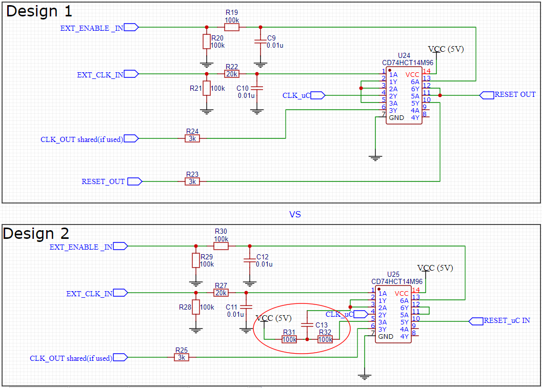
 I have an application where i want to use the external clock signal (around 1kHz) with my microcontroller. I am interested in positive edge of the clock which will be detected by microcontroller. I also want to be able to keep "boosting" this clock so that another circuit (another copy of same circuit) can re-use the same clock signal if needed (like cascading ).
My solution: "Design 1" where I just send the inverted clock signal from schmitt trigger (HCT14M) output (1Y) to two of its inputs (2A & 3A). One of the output (2Y) will be used by my microcontroller and another output(3Y) can be used as "Clock Out" for external circuits. I am using this schmitt trigger because:
- The External CLOCK OR ENABLE pulse can be greater than 5V,( max around 10V). Hoping the 20K/100K series resistor will limit the input current <20mA and will be accepted by the schmitt trigger. This will also act as voltage translator. Datasheet mentions that "The input and output voltage ratings may be exceeded if the input and output current ratings are observed.". Since Input/output clamp current is 20mA, I guess this is okay??
- I also want to use this schmitt trigger to maintain the CLOCK shape when being shared with other circuits and it'll also act to "boost" it for cascading.
However, I saw another circuit (Design 2) which essentially is using the CLOCK sharing like I just mentioned. It used the same Schmitt trigger. However instead of just passing the inverted CLOCK pulse (1Y) to another schmitt trigger input, it seems they sent the inverted clock signal through a capacitor (unsure about its value). Then used 100k pullup resistor and another 100K resistor in series before sending it to the schmitt trigger input. Finally used this output for cascading. From what I know, you can add capacitor in series to use as edge detector. Also one of the 100K resistor is being used as pullup so that the output is normally LOW. Which makes sense. I guess.. I want to understand this setup as a whole.
My questions:
- How is "Design 2" CLOCK boost circuit better? is it better than my simple Design 1 ?
- Using series resistors 100k,20K for ENABLE & CLOCK signals will it allow me to use higher voltage signals (>Vcc) as input sources to my schmitt trigger ? if so, what happens to the "HIgh level" and low level input voltages. Will they remain the same or will it change depending on the input voltage levels?
