1
\$\begingroup\$

Reference

enter image description here

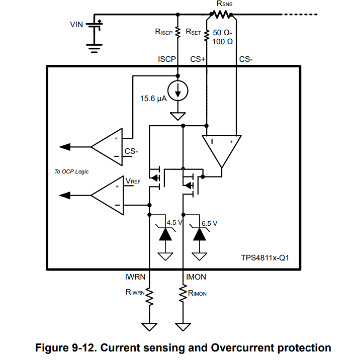
  1. I couldn't understand the implementation of current monitoring for this IC. "The current source at IMON terminal is configured to be proportional to the current flowing through the RSNS current sense resistor."

Per my observations, there is no current source at the IMON terminal.

  1. VOS_SET input referred offset. What is the need for this & what does it mean?

enter image description here

  1. VSNS to VIMON scaling. What is meant by scaling in this context?

  2. Why is the clamp set to 6.5V? As per the given range VVS -0.5V (Upper bound). VVS can go up to 80V or close to it as per the datasheet.

A simplified breakdown of the working would help me immensely.

\$\endgroup\$

2 Answers 2

2
\$\begingroup\$

Per my observations, there is no current source at the IMON terminal.

Actually there is but you didn't recognize it. You probably accept that CS- will be at a slightly lower voltage than the input side of the shunt resistor (\$R_{SNS}\$) due to load current. Does that make sense so far?

Well, in order to get the op-amp into stability (Cs- = CS+), the voltage at CS+ can be "dragged-down" to equal the voltage at CS- by activating the p-channel MOSFET and taking some current from \$R_{SET}\$, through the MOSFET and down to ground via \$R_{IMON}\$.

Does that make sense and, do you see that this all happens automatically within a negative feedback loop. Hence, the current source at IMON is the op-amp and MOSFET working together.

Of course, that current taken from the CS+ pin flows to ground through \$R_{IMON}\$ and, the voltage produced is proportional to the real load current through the shunt resistor \$R_{SNS}\$.

  • Scaling refers to the current through \$R_{IMON}\$ compared to the actual current through \$R_{SNS}\$.
  • The offset of the op-amp represents an error factor. Ideally it would be 0 μV but nothing ever is that good.

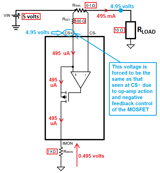
It might help if you concentrated on the crucial parts of the circuit that dictate performance and, put some example numbers on things: -
enter image description here

\$\endgroup\$
11
  • \$\begingroup\$ Since the output of the op amp is driving the gates of the PFET. What would be the gain of the op amp in this scenario as it is different from the conventional feedback resistor configuration. Would it be like R(ON) of the fet? Didn't understand the scaling thing, what significance does it hold for the proper functioning? \$\endgroup\$
    – Harkirat
    Commented Apr 28, 2023 at 7:04
  • \$\begingroup\$ You might be missing the point here. The gain of the op-amp is whatever it needs to be to overcome the MOSFET gate threshold voltage and apply enough extra gate voltage so that the voltages at CS+ and CS- balance. \$\endgroup\$
    – Andy aka
    Commented Apr 28, 2023 at 10:42
  • \$\begingroup\$ I did understand the use of negative feedback of the op amp via the PFETs. Which forces a virtual short condition, thereby CS+ = CS-. I got the current source part. Is the scaling term to ensure that I(IMON) is roughly equal to I(SNS)? \$\endgroup\$
    – Harkirat
    Commented Apr 28, 2023 at 13:19
  • \$\begingroup\$ @Harkirat IMON is very much less than ISYS. Think about RSYS; it's usually an ohm or less then, think about its equivalent partner on the other lead RSET; it is 50 to 100 ohm and, the op-amp therefore tries to take an appropriate current through RSET to get the exact same volt drop across RSET as there is across RSNS; this is the scaling I believe you are talking about. Think of the circuit as a Wheatstone bridge where the op-amp tries to make the bridge balanced and, think about the much higher impedances down the RSET branch compared to the RSNS branch. The RSNS branch includes the load. \$\endgroup\$
    – Andy aka
    Commented Apr 28, 2023 at 13:23
  • 1
    \$\begingroup\$ I made a slight numerical rounding error in that picture that I'll fix. \$\endgroup\$
    – Andy aka
    Commented Apr 28, 2023 at 16:05
2
\$\begingroup\$

The op-amp connected to the sense resistor will drive the gate of the FET to bring the - terminal to the same potential as the + terminal. (Negative feedback plus high gain.)

In doing that it forces the voltage across the sense resistor to be equal to the voltage acoss Rset. The current in Rset can only flow through the body of FET (Since the op-amp inputs are high impedance) and will generate the IMON voltage by flowing through Rimon. (There's an offset and gain factor, see datasheet.)

The block diagram is highly simplified, so doesn't reflect the detailed working of the device. The zener clamps shown are likely cascode devices to improve compliance, not actual zeners. Since the Imon and Iwrn pins are referenced to ground, there's no reason for those pins to require a high voltage, and to do so would complicate the IC design and increase the cost.

\$\endgroup\$

Your Answer

By clicking “Post Your Answer”, you agree to our terms of service and acknowledge you have read our privacy policy.

Not the answer you're looking for? Browse other questions tagged or ask your own question.