0
\$\begingroup\$

So as I understand it, with a resistive load, when the voltage at the gate relative to the source is increasing from VTH to VGP, it seems that the value of VGP is the voltage at which the current through the drain goes from 0 to the full load current. Following this, during the miller region of the turn-on process, the gate current is used to charge the reverse transfer capacitance (Crss). VDS is decreasing from VDD + VBD to ID * RDS(ON). Thus the voltage across Crss (gate-to-drain capacitance) changes from {(VDD + VBD)−VGP} to {(ID * RDS(ON)) − VGP}. For reference, I've been using the formulas provided by this application note by ON Semiconductor located here: https://ghioni.faculty.polimi.it/pel/readmat/AND9083.pdf

So to find the charge to bring the voltage at the gate (relative to source) from 0 to VGP is to take the integral of the capacitance curve from VDD to VDD minus VGP using CISS. Then, to find the charge for the miller region, I would solve for the integral using the CRSS curve from (VDD minus VGP) to zero since the voltage across CGD is already charged to VGP, then for the polarity change in which the voltage at the gate becomes higher than the voltage at the drain, I would solve for the integral from VGP to 0.

For the following example, I'll be using the datasheet for this N-channel mosfet here: https://datasheet.lcsc.com/lcsc/2201121830_Jiangsu-JieJie-Microelectronics-JMSL0302AU-13_C2938488.pdf

Additional Conditions

-Assume a perfect mosfet, with zero drain to source resistance when it's on, and an infinite amount when it's off

-Mosfet is being used as a low-side switch with the gate to source voltage difference becoming higher than the voltage difference across drain to source when the mosfet is on

-Mosfet is driving a resistive load

Note, for the sake of simplicity, for the value of when VDS = RDS(on) * I(load), I'll just be using 0 instead.

What I've been doing is creating a function by curve fitting then plugging in the values which I've highlighted in bold.

I can show my work and my process for determining these formulas if needed, but basically used y=a(x-h)^(1/3)+K and used the value of the capacitance at zero VDS for my Y-intercept and then used the capacitance value from each curve with VDS at 30 volts to solve for a.

T1-T2

AKA VGS @ 0 to VTH & VTH to VGP


FUNCTION FORMULA (using CISS):

y=-1.5329443e-10x^(1/3)+3.344978165E-9

INTEGRAL:

((((-1.5329443e-10((VDS)^(4/3)))/(4/3))+(3.344978165E-9(VDS)))

-

(((-1.5329443e-10((VDS-VTH)^(4/3)))/(4/3))+(3.344978165E-9(VDS-VTH))))

+

((((-1.5329443e-10((VDS-VTH)^(4/3)))/(4/3))+(3.344978165E-9(VDS-VTH)))

-

(((-1.5329443e-10((VDS-VTH-(VGP-VTH))^(4/3)))/(4/3))+(3.344978165E-9(VDS-VTH-(VGP-VTH)))))

T2-T3

AKA Miller region: the fall of the drain voltage while holding the charge voltage across CDS at VGP


FUNCTION FORMULA (using CRSS):

y=-1.6441226e-10x^(1/3)+5.28E-10

INTEGRAL (Two Parts):

Part One: When the voltage across CGD is more positive on the Drain side relative to VGP

((((-1.6441226e-10((VDS-VGP)^(4/3)))/(4/3))+(5.28E-10(VDS-VGP)))

-

(((-1.6441226e-10((0)^(4/3)))/(4/3))+(5.28E-10(0))))

+

Part Two: When the voltage across CGD is more positive on the Gate side and the drain side is more negative relative to VGP

((((1.6441226e-10((VGP)^(4/3)))/(4/3))+(5.23606557377e-10(VGP)))

-

(((1.6441226e-10((0)^(4/3)))/(4/3))+(5.23606557377e-10(0))))

With these formulas I would add the results the above calculations would produce (plus the charge from VGP to the full gate drive voltage), then divide that by (V(GateDrive)/R(tot)) to get the amount of time the turn-on process would take.

Now here's where I am confused, the first time current is able to flow through the drain to source (not counting any leakage) after VTH, till the point that the current through the drain reaches the full load current at the end of the miller region when VGS is finally able to become charged beyond the gate plateau, the above calculations only hold true if CDS is not taken into account.

Excluding any other parasitic influences the rest of the circuit presents from traces and whatever the gate driver presents, and strictly analyzing the mosfets own parasitics, the fall of VDS won't happen at the rate the gate driver can produce a change in voltage across the Gate to Drain if CGD is not the only factor influencing the drain at that time. When CGD is releasing it's charge from Vin through the drain to 0, so is CDS in parallel. But if I were to find a function to represent the COSS curve, and then solve for the integral with the same process I used for part one of T2-T3 above, it'd be inaccurate because that would look like I'm trying to charge CDS as well.

So to close this wall of text,

(1) Since the capacitance of CRSS (and all the other ones in a mosfet) are dynamic and dependent on the voltage at the drain, how would I mathematically solve for the charge on CGD needed to get through the miller region when the voltage on the drain is also being influenced by the parallel discharge of CDS?

(2) How do I determine the amount of current that will be flowing through the drain to source if the output capacitance of the mosfet is discharging and is also producing current from the charging of CGD? How do I account for the current flowing through my load for every change on the drain voltage?

(3) If the current through the load is relatively low (ILoad<0.1 mA) is it possible for the output capacitance to be large enough that at some point during the turn-on process the current through the drain to source will be larger than my desired full load current? What impacts will this have on determining at what voltage VGP occurs if that happens?

\$\endgroup\$

1 Answer 1

0
\$\begingroup\$

Don't worry, there are much simpler ways to handle this!

First of all, curve fitting is something one needs to do carefully. Depending on purpose, of course. For example, all the fractional powers in your expressions are non-analytic at zero. Their derivatives (or higher) also may not match up. So composing a piecewise function in this way may prove awkward, and hard to use.

If you're just doing it to plot the curve (I suppose to better interpolate some data?), that's fine.

If the expressions are to be used in SPICE, analyticity helps, because it performs symbolic (if possible) differentiation of expressions, in order to calculate the next time step (numerical integration). Smooth functions like polynominals and exponents are best; rough functions like piecewise-linear, division, and fractional (or decimal) exponentiation, are less preferable. Rough functions should be used carefully, to give the simulator the best chance of finding a low-error solution quickly. For example, bounding the input and output of the function (preferably with other continuous functions, or circuit nodes).

Also a useful trick, make use of built-ins where you can. SPICE diodes are very fast to execute, and numerically stable (they're not interpreted expressions but use internal and optimized code), and make excellent exp/log functions, clamping, etc.

As for gate charge -- the simpler methods are either more empirical (i.e. refer to datasheet curves) or -- for lack of a better term, thermodynamical, in that you only need to know the start and end points, and the totals between them. Which is also to say, the exact particulars inbetween aren't very interesting, so don't worry about it.

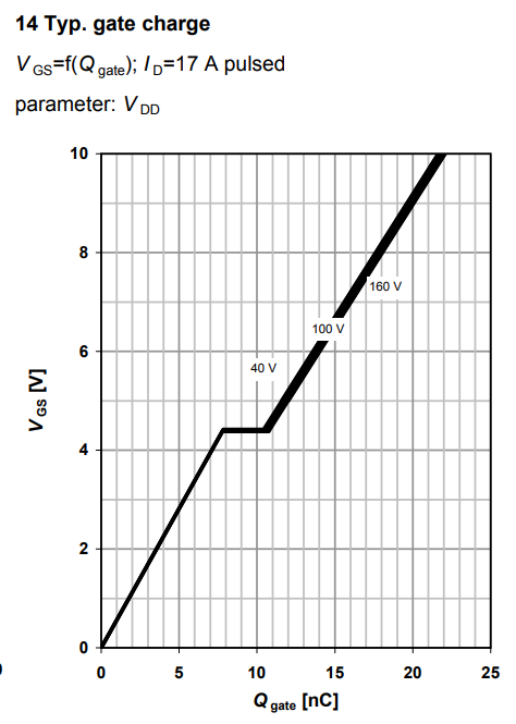
For example, consider a typical gate charge curve: IPP320N20N3,

Gate charge curve

Notice how little it varies with initial VDS. The variation of course depends on type, but modern transistors are offering impressively low Crss, particularly at high VDS. For design purposes, simply use the worst-case (maximum) gate charge, and that'll be that. Drain rise/fall time will be a modest fraction of gate fall/rise time; how much depends on load phase as well as device characteristics. (For resistive load, the times are as given in the datasheet.)

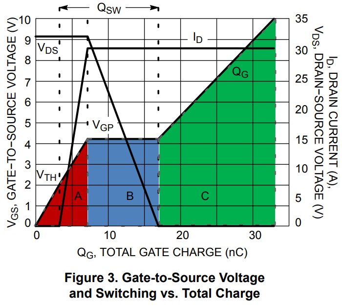
Especially against older reference material (AND9083 I don't think is that old), beware of facts that are no longer relevant. Consider Fig.3 for example:

AND9083 Fig.3 Gate-to-Source Voltage and Switching vs. Total Charge

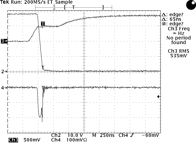
I measured these waveforms on a IPA60R120P7:

IPA60R120P7 turn-on waveforms

Ch2 and 3 have 10x probes, so that's 8V VGS(on), and 400V bias to the drain. (Ch4 is VDS derivative, for reference.)

Now, this is a much higher voltage device, using SJ (SuperJunction) technology*, so its C(VDS) curve is especially exaggerated; it's also a capacitive load, not inductive. But it shows how small QDG is, over the bulk of the voltage range. In particular, notice how much of the Miller plateau is at low VDS (under 30V).

*SJ is currently applicable to devices 200V and above, I think. It may eventually filter down to lower voltages, though 30V range devices like in the appnote seem unlikely. Lower voltages are more conventional VDMOS, as far as I know; just with ever tighter optimization.

Another wrinkle with the appnote figure is it's a hard-switched inductive test. Yet ID is not shown peaking at all above IL (reverse recovery current), nor VDS holding still (or bouncing because of loop inductance) during recovery.

The giveaway is, the curves are drawn from straight line segments; it's a cartoon figure, which applies when everything is ideal (in this case, ideal diode, constant gm FET, fixed capacitances and no inductances). In reality, the curves will be skewed considerably when VDS is low.

To similarly summarize:

  1. Crss can be lumped in as a total (see datasheet parameters and curves). Charge is charge, so it doesn't depend upon CDS, but do mind Coss = CDS + Crss, so it serves as part of output capacitance and therefore dVDS/dt depends on load current as well as gate current during the Miller plateau.

  2. Unless you're forcing the FET into linear range*, there's simply enough excess ID to discharge both. CDG becomes the controlling factor (at least, to the extent that it's controlling slew rate, given how wildly it changes), and load current takes up the rest.

    Note that, as load current rises, VGS must rise, because that determines ID (total). A substantial resistive load will therefore have a sloped Miller plateau.

    *Traditionally called (FET, current) saturation, but I would urge people to avoid that use, which conflicts with the common meaning (voltage saturation). I add this note for clarity.

    *Anyway, in linear range, VDS stops falling, so capacitor currents stop too, making them irrelevant.

  3. The system is tightly coupled (CDG and CDS are inside the device) so there's no overcompensation effect to happen here. At least, not at any modest rate of change; arguably maybe gate oscillation counts as this, but that's also better described as a conventional oscillator.

    In any case, ID eventually drops as the device saturates**, and no amount of excess VGS can change that. Since we're talking capacitances here, you can only draw current from them for so long, and eventually VDS runs out and no more current can be drawn than whatever load current is connected.

    **Voltage saturation.

\$\endgroup\$

Your Answer

By clicking “Post Your Answer”, you agree to our terms of service and acknowledge you have read our privacy policy.

Not the answer you're looking for? Browse other questions tagged or ask your own question.