1
\$\begingroup\$

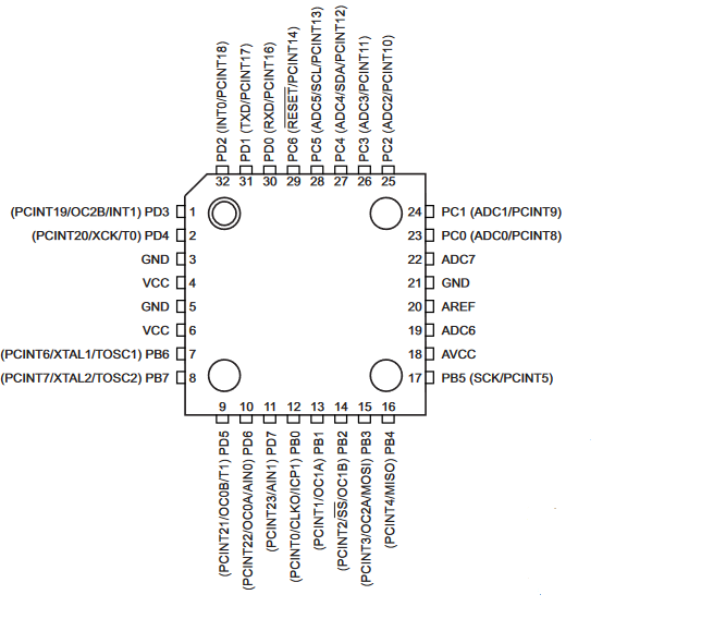
I have went through numerous times where the Vcc pin is shorted with the GND pin causing damage to the entire microcontroller, for example, pins 3 and 4 and pins 5 and 6 in the ATmega328P :

ATmega328P pinout

Image source: Microchip - ATmega48A/PA/88A/PA/168A/PA/328/P datasheet

Why do the engineers always place the Vcc pin next to the GND pin?

\$\endgroup\$
4
  • 1
    \$\begingroup\$ John Sall - Hi, You said: "the Vcc pin is shorted with the GND pin causing damage to the entire microcontroller" You have referred to similar terminology in other recent repair questions. However you seem to be reversing cause & effect. If an MCU has an internal short between Vcc (or Vdd) & Gnd, that did not cause damage to the MCU. Instead it's internal MCU damage (e.g. caused by EOS etc.) that caused the Vcc to Gnd short which you can measure. || All that is assuming the MCU has that internal short, as some of your previous questions were unclear about where on the PCB the short was. \$\endgroup\$
    – SamGibson
    Commented Jul 8, 2023 at 15:44
  • 1
    \$\begingroup\$ John Sall - Hi, Please remember the site rule which requires that when a post includes content (e.g. text, image, photo etc.) copied or adapted from elsewhere, that content must be correctly referenced. As a minimum, the source webpage or PDF etc. should be linked (see that rule regarding references for books / articles etc.). In order to help you, I found what I believe to be a source PDF link & added it for you. For the future, please remember it's your responsibility to do that :) To remind yourself of the main site rules, please see the tour & help center. Thanks. \$\endgroup\$
    – SamGibson
    Commented Jul 8, 2023 at 15:51
  • 2
    \$\begingroup\$ The question is based on false assumption. If VCC and GND are shorted at the MCU pins, it cannot damage the MCU, because there will be 0V over MCU VCC and GND pins, and no current passes through the MCU. Now, why MCUs have GND and VCC next to each other is a good thing and does not relate to short circuits in any way. \$\endgroup\$
    – Justme
    Commented Jul 8, 2023 at 16:07
  • \$\begingroup\$ @Justme - Hi, "The question is based on false assumption" Agreed, that's what I tried to explain to the OP in my first comment above. Although it's a valid question, in context this looks like an "XY-problem". \$\endgroup\$
    – SamGibson
    Commented Jul 8, 2023 at 16:12

3 Answers 3

7
\$\begingroup\$

Adjacent pins allow very short paths to the critical bypass capacitor.

You always want the DC voltage between Vdd and GND to be pure DC with no glitches or ripples. Longer paths between bypass capacitor(s) and these pins have inductance - which decreases the bypass capacitor's effectiveness. Current pulled by the processor internal switches on these paths are inherently glitchy, which allows any inductance to cause variations.

You'll notice that another critical pin AREF also has an adjacent GND pin. Same reason - you want voltage between AREF and GND to be un-varying.

If you're planning PCB layouts, add these bypass capacitors first, and put them as close as possible to the chip pins.

\$\endgroup\$
5
\$\begingroup\$

Because it minimizes the parasitic inductance of the power supply. Or in other words: It maximizes how quickly the part can draw energy from the power distribution network (the bigger the space between Vcc and GND, the bigger their inductance).

How important minimizing parasitic inductance is, depends on the part. Some heavily switching parts like big FPGAs might need a lot of energy in a very short period of time. Such parts usually have many more such Vcc-GND-pairs.

\$\endgroup\$
2
\$\begingroup\$

TLDR: With regards to component package design, there are more important things to consider than whether or not 2 pins will short together during PCB assembly.

I wouldn't say that the VCC and GND pins are almost always next to each other because it really depends on the component, but it really helps with same layer decoupling when they are.

It helps with placement, ensures that you can route healthy current paths, and prevents blocking the fanout of other signals that get stuck between the power/ground pins. That's probably as far as it goes with packages like the ATmega328P if we don't dive into the details of the internal die, but with large BGAs, it's necessary to put VCC and GND next to each other to allow decoupling on the back of the board without forcing the engineer to use very small footprints. For some power supplies, it's about minimising the eddy currents and improving EMI.

"Why do the engineers always place the Vcc pin next to the GND pin?". The target customer for most electronic components would typically be dealing with high volumes and/or high-quality professional assembly where shorting between pins is generally caught in a number of ways. I don't think the risk of shorting pins would be a consideration.

\$\endgroup\$
0

Your Answer

By clicking “Post Your Answer”, you agree to our terms of service and acknowledge you have read our privacy policy.

Not the answer you're looking for? Browse other questions tagged or ask your own question.