6
\$\begingroup\$

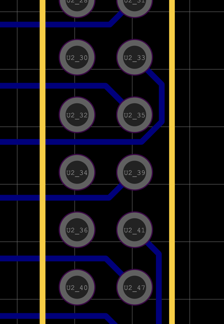
I have made a design and I am now creating a PCB board for the first time. I ended up using the "Auto Route" feature on the EASYEDA software because I have to make a lot of connections and it was kind of hard make the connections myself in such a small area.

Because of this the auto route feature ended up putting PCB traces inbetween the 2.54 pitch through hole connectors shown in the image below:

enter image description here

Is this okay? Or does that not provide enough clearance? I'm pretty new at designing a PCB so any help would be appreciated!

\$\endgroup\$
2
  • 3
    \$\begingroup\$ "Or does that not provide enough clearance?" - it provides no less clearance than whatever clearance you specified in your PCB's design rules. \$\endgroup\$
    – brhans
    Commented Jul 11, 2023 at 0:31
  • \$\begingroup\$ What signals are there on the connector? How much voltage? Required clearance also depends on voltage - or in other words - on the level of isolation that you need. So the answer about clearance can't really be given - but what you show looks not uncommon for manufacturing. \$\endgroup\$
    – datenheim
    Commented Jul 11, 2023 at 18:23

3 Answers 3

13
\$\begingroup\$

Running tracks between pads on 0.1" (2.54 mm) spacing was common practice with through-hole parts - IC leads were on 0.1" spacing.

If I recall correctly, I normally used .060" (1.5 mm) pads and .012" (0.3 mm) tracks - that allowed .014" space between track and pad.

\$\endgroup\$
3
  • \$\begingroup\$ .060" + 0.12" + 2 * .014! = .100" You recall it correctly. \$\endgroup\$
    – Uwe
    Commented Jul 11, 2023 at 13:53
  • 2
    \$\begingroup\$ Looking at the OP's picture, I think the problem isn't clearance, it's track size. Those look thin enough that they might have issues getting it made. Probably not if they go to a good PCB manufacturer, but if they're planning on going old-school and making it themselves, they're going to have problems with tracks that thin. \$\endgroup\$
    – Graham
    Commented Jul 11, 2023 at 14:55
  • \$\begingroup\$ @Graham That, and there is margin to make the traces more than twice as wide. \$\endgroup\$
    – Kaz
    Commented Jul 12, 2023 at 18:56
12
\$\begingroup\$

If it meets the trace width and clearance design rules, then it will be manufacturable.

Assuming you don't have any weird impedance control or high frequency (>> 100 Mbps) signals, then in all likelihood it will work just fine as routed.

2.54 mm pitch headers usually have a pretty large amount of space between the pins, so it is pretty common to find signals routed in between them.

\$\endgroup\$
6
\$\begingroup\$

You need to satisfy the constrains set by the PCB fab.

The hole has to be in an acceptable range to accept the connector pin.

The annular ring has to be at least as big as the minimum the fab specifies, and may have to be bigger in order to provide mechanical strength depending on your requirements- you are free to use non-circular pads if you want to for mechanical reasons.

The clearances on either side of the pads have to be large enough to be manufactured and they have to meet any other requirements you may have (such as for elevated voltages)

The trace has to meet the minimum trace width requirement for fabrication and to meet any other requirements you may have (they can be necked down in close proximity to the pads in order to sneak through if you need wider traces for current-carrying or trace resistance reasons.


To pick an example, say you are using this Molex connector and JLC PCB design rules.

The recommended hole size is 1.02mm (from the linked drawing).

The minimum track to via spacing is 0.2mm and the minimum trace width is 0.127mm. Let's say you use 0.2mm for all three (about 8 mil trace and space) and, so you need 0.6mm for the trace and two spaces.

That means the pad can be 2.54mm - 0.6mm = 1.94mm diameter.

The minimum annular ring is 0.13mm so you can have a pad of minimum 1.02 + 2* 0.13 = 1.28mm diameter so there's plenty of margin.

You might choose to use 1.9mm diameter pads to give good strength.

Other manufacturers will have similar capabilities, for example OSHPARK does not allow 0.127 mm traces (0.1524 mm minimum) and there are some other small differences but the above choices (0.2mm trace width and clearances and 1.9mm pad) will also be manufacturable by them. It's good to avoid using the absolute minimum clearances, annular ring and trace widths because it reduces manufacturability and may reduce the choices of fabs without tweaking the design. That goes double for dimensions that appear in many places on the board (such as trace widths and clearances for most of your traces, annular ring and drill diameter for vias, and clearances around copper pours).

\$\endgroup\$

Your Answer

By clicking “Post Your Answer”, you agree to our terms of service and acknowledge you have read our privacy policy.

Not the answer you're looking for? Browse other questions tagged or ask your own question.