0
\$\begingroup\$

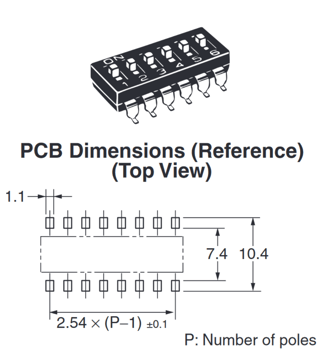
Here is excerpt from datasheet for the A6S-4101-H.

enter image description here

I need two rows of pads. The distance between (center of) pads in a row is 2.54mm. The distance between the (center of pads) two rows is 8.9mm. Each pad size is 1.1mm x 1.5mm. Now I want to use a wizard from Altim to make this footprint but am not sure what option to choose. This package is just called SMD/SMT. But such a "general purpose SMD/SMT" package does not exist in the list in either of the two wizards that exist in Altium.

\$\endgroup\$
3
  • 2
    \$\begingroup\$ Use the SOIC tool. \$\endgroup\$ Commented Jul 15, 2023 at 22:21
  • \$\begingroup\$ I spent sometime and created the footprint manually, it took a while but its done. I will keep this in mind for next time. \$\endgroup\$
    – quantum231
    Commented Jul 15, 2023 at 23:10
  • 1
    \$\begingroup\$ The pin spacing matches a common through-hole DIP pattern very closely - I'd copy a DIP footprint, then change the through-hole pads to surface mount. \$\endgroup\$ Commented Jul 16, 2023 at 5:51

1 Answer 1

1
\$\begingroup\$

If the 3d is important to you (probably is), the best options are either use the SOIC and live with it or improve it.

The pro's of using the IPC compliant footprint generator:

  • Quick and easy
  • Gives you a black box 3d(still better then none!)
  • Creates all the appropriate layer automatically

But it won't (and you might want to correct those):

  • Import the proper 3d from a 3rd party website
  • Change the silkscreen for something more significant

Side note, many switch definition don't follow the standard pin definition of ic:

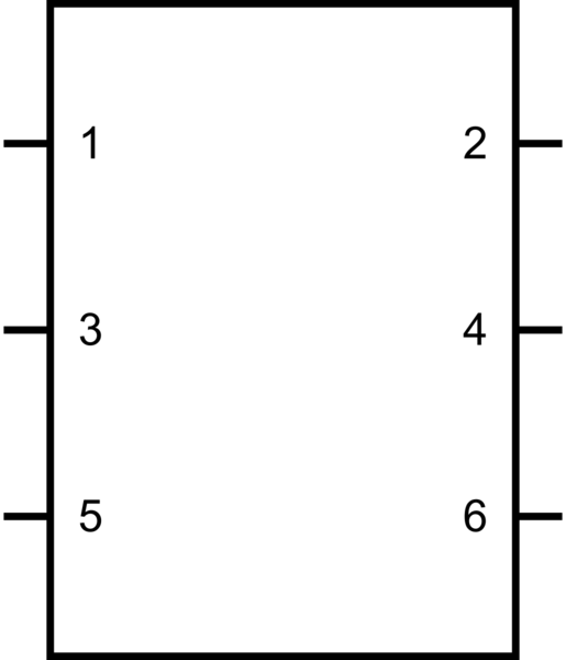
schematic

simulate this circuit – Schematic created using CircuitLab So ensure that it fits your schematic!

\$\endgroup\$

Your Answer

By clicking “Post Your Answer”, you agree to our terms of service and acknowledge you have read our privacy policy.

Not the answer you're looking for? Browse other questions tagged or ask your own question.