1
\$\begingroup\$

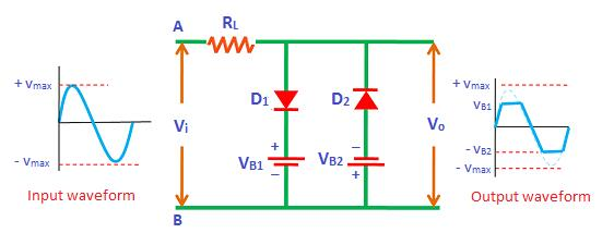
What is the difference between clamp circuit and clipping circuit? TVS diode clamp property and clamp circuit is same or not? I am confused because of some pictures. Please explain this confusion.

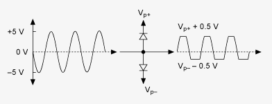
This is TVS diode clamp property.

enter image description here

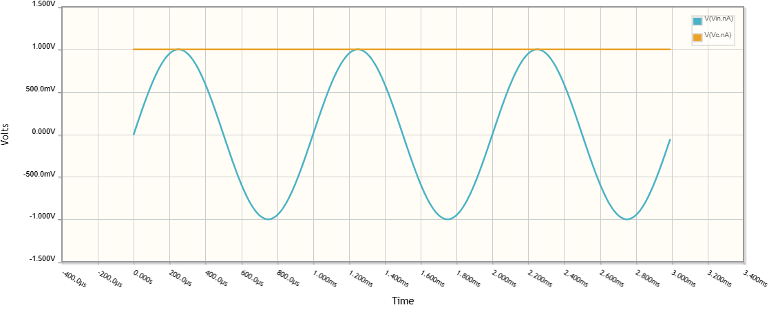
This is a clamper circuit

enter image description here

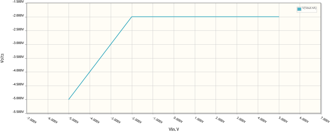
This is clipper circuit

enter image description here

What is the clamper meaning? TVS diode clamper and clip circuit is same or not? What is the real difference in clamp function between first and second circuit?

\$\endgroup\$
3
  • \$\begingroup\$ Please explain in depth. \$\endgroup\$
    – bb0667
    Commented Jul 16, 2023 at 15:18
  • \$\begingroup\$ bb0667 - Hi, Please note the site rule which says that when a post includes content (e.g. text, image, photo etc.) copied or adapted from elsewhere, that content must be correctly referenced. The source webpage or PDF etc. should be linked as a minimum (references for books / articles should include title, author(s), publisher, edition, page numbers etc.). Therefore please can you edit your question to include the link(s) for the original source(s) for each of those images. Thanks. \$\endgroup\$
    – SamGibson
    Commented Jul 16, 2023 at 16:08
  • 1
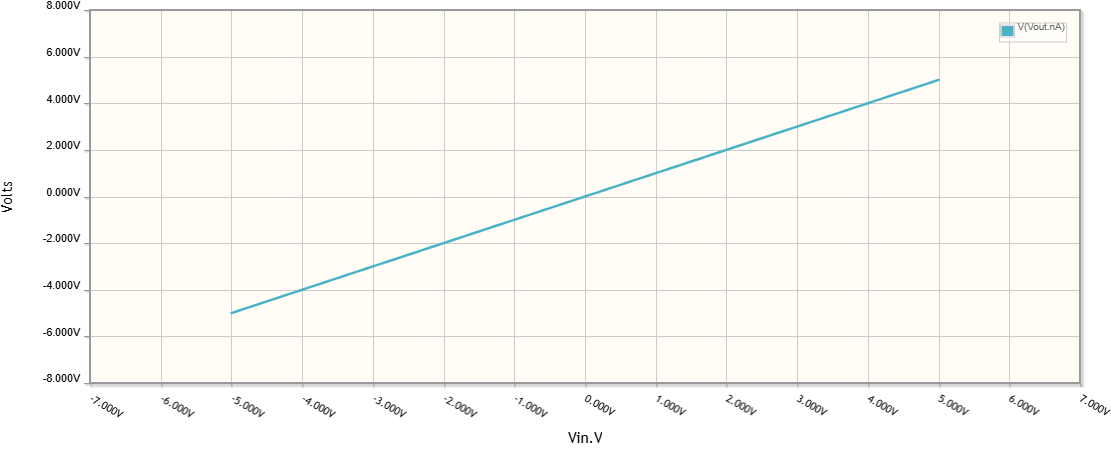
    \$\begingroup\$ The first circuit seems to be erroneous: it shows two diodes clamping in the same direction, one to a negative voltage which therefore dominates, and no clamping in the negative direction. \$\endgroup\$ Commented Jul 16, 2023 at 16:45

4 Answers 4

1
\$\begingroup\$

The middle circuit is more likely, or more properly, called a "DC restore" circuit. At least when the RC time constant is much longer than the period of the signal.

\$\endgroup\$
0
\$\begingroup\$

I would use the term "clipper" for a circuit that limits its output at some high or low level or both, but otherwise leaves the output unchanged from the input.

I would use the work "clamp" for a circuit that adds an offset to its output such that the output is never below (or alternatively above) a certain value.

Thus, as I use the terms, your first circuit is a bipolar clipper, not a clamp. It is unfortunate that it is sometimes called a clamp, because that confuses the distinction between clipper and clamp. But I cannot control other people's use of words.

The 2nd and 3rd circuits, I would label as you have done in the question.

The 2nd is a clamp. It shifts the output so that it never negative.

The 3rd is a clipper. It leaves the output un-shifted, but clips off excursions that are above or below certain limits. However, you will sometimes see the diodes in such a circuit referred to as "clamping" diodes. Again, it is confusing, but little can be done to enforce particular usages.

\$\endgroup\$
0
\$\begingroup\$

Your first and last circuits are both clippers - they chop off the top and bottom of the input waveform.

A clamp circuit will hold some part of the input waveform at a certain DC level, but keep the full input waveform.

\$\endgroup\$
0
\$\begingroup\$

There seems to be a confusion in the question. It is comparing two different types of diode circuits: a simple DC clipper and a more complex AC+DC clamper. Let's break them down.

Clipper circuit

Basic idea

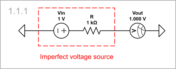
If we connect an ideal voltage source with zero internal resistance in parallel with a non-ideal voltage source with some internal resistance, the voltage across the parallel combination will be equal to the voltage of the ideal voltage source. Let's illustrate this idea with conceptual circuit diagrams.

No clipping: In the picture below, a 1 V input voltage source Vin and a 1 kΩ resistor R in series form an imperfect voltage source. Since there is no load connected (only an "ideal" voltmeter), no current flows, there is no voltage drop across the resistor, and the output voltage is equal to the input one.
schematic

simulate this circuit – Schematic created using CircuitLab

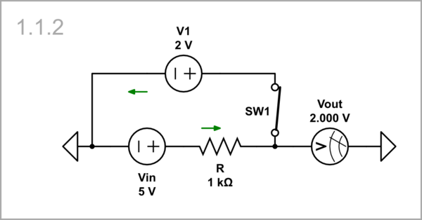
Positive clipping: Now, imagine that when the input voltage reaches the voltage (2 V) of the positive ideal source, the two sources are connected via a switch SW1 in parallel. The output voltage stops changing and is fixed at 2 V. Think of it like this: there is a "battle" between two voltage sources, and the ideal V1 always wins.
schematic

simulate this circuit

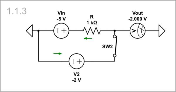
Negative clipping: Similarly, imagine that when the input voltage reaches the voltage (-2 V) of the negative ideal source, the two sources are connected via a switch SW2 in parallel. The output voltage stops changing and is fixed at -2 V (the ideal source V2 wins the "battle").
schematic

simulate this circuit

Implementation

In the practical circuit below, the switches are implemented with diodes.

Missing resistor: The trick above was that we intentionally "weakened" the input source by connecting a resistor in series with it, so that it always lost the battle with V1 and V2. However, in the OP's circuit, there is no such resistor, and this is the first mistake. As a result, a huge current flows through the parallel sources.
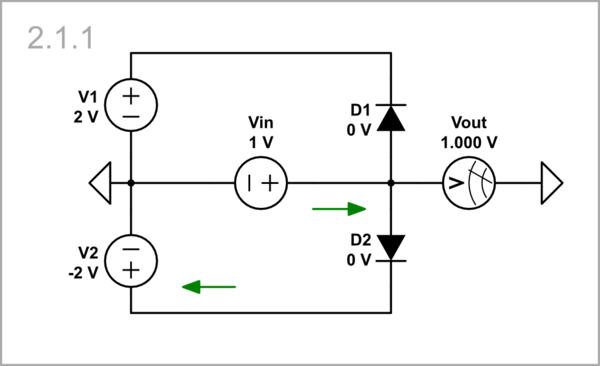
schematic

simulate this circuit

STEP 1.1

Incorrectly placed diode D2: The second mistake, as @Tim Williams also noticed, is the incorrect orientation of diode D2. As a result, at Vin > -2 V, D2 is always on, and D1 is never on (wrong operation).
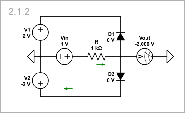
schematic

simulate this circuit

STEP 1.2

Correctly placed diode D2 (clipper circuit 3): So, let's flip vertically D2...
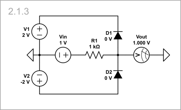
schematic

simulate this circuit

... to obtain the accurate transfer function.
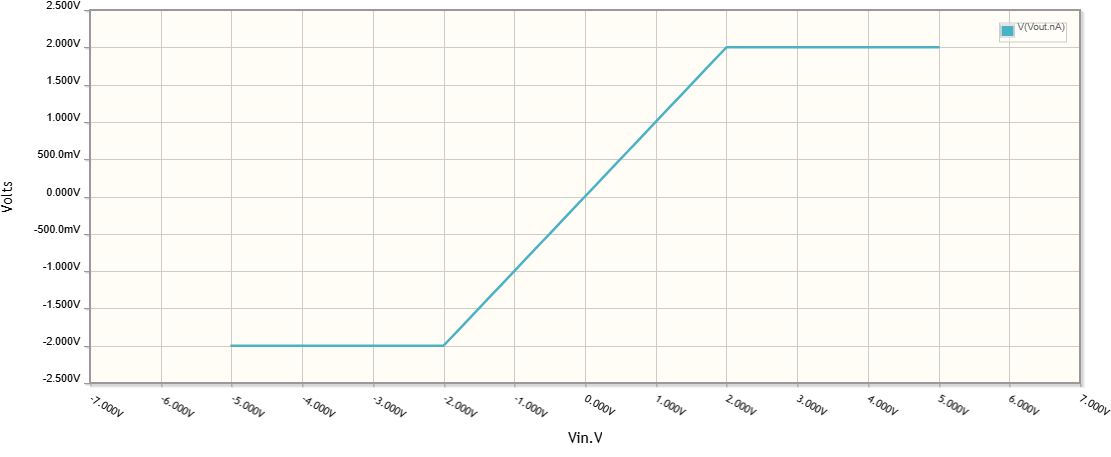
STEP 2.1

Clamper circuit

Despite being revered as a unique and complex design...

Diode rectifier

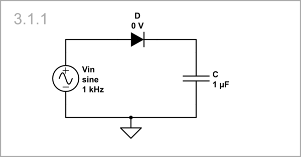
... this circuit is essentially a basic half-wave diode rectifier with a filter capacitor.

Real circuit: The capacitor charges during each positive half-wave...
schematic

simulate this circuit

... and we use its voltage as the output DC voltage.
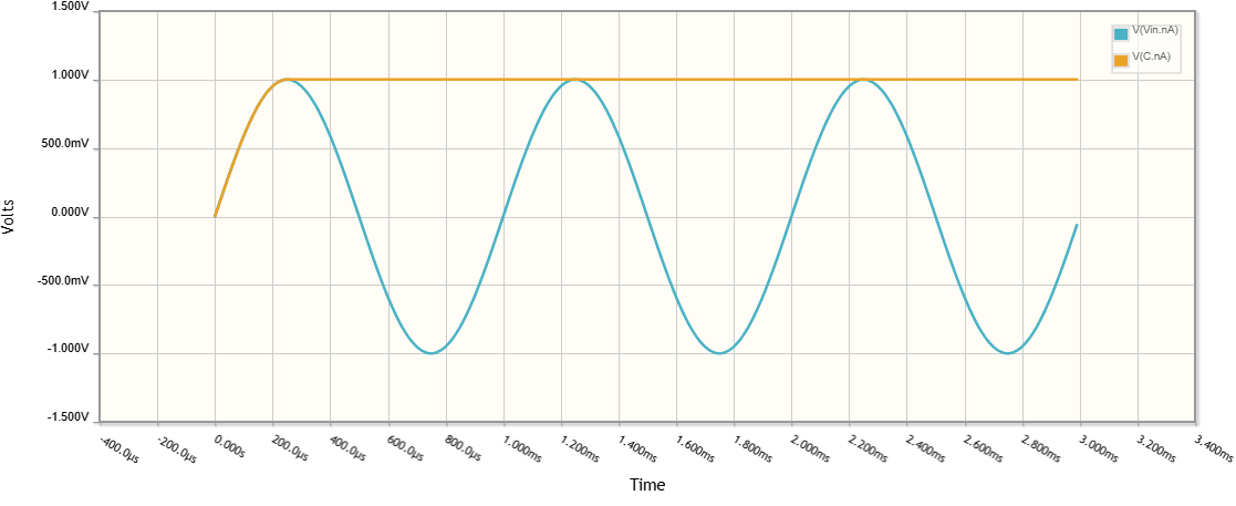
STEP 3.1.1

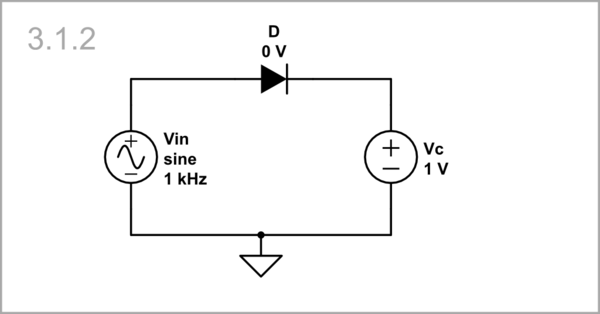
Conceptual circuit: So, we can think of the capacitor as a constant voltage source.
schematic

simulate this circuit

STEP 3.1.2

Diode clamper

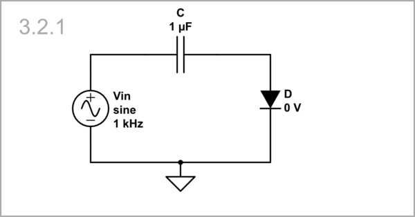
Here, the diode and capacitor are swapped.

Real circuit: We take the voltage across the diode as the output. In an ideal case, the diode is off...
schematic

simulate this circuit

... and this is actually the sum of the input AC voltage and the constant DC voltage across the capacitor.
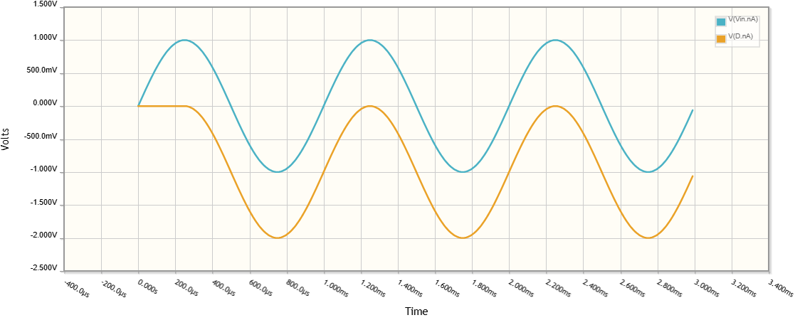
STEP 3.2.1

Conceptual circuit: As above, we can think of the capacitor as a constant voltage source connected in series to the input voltage source...
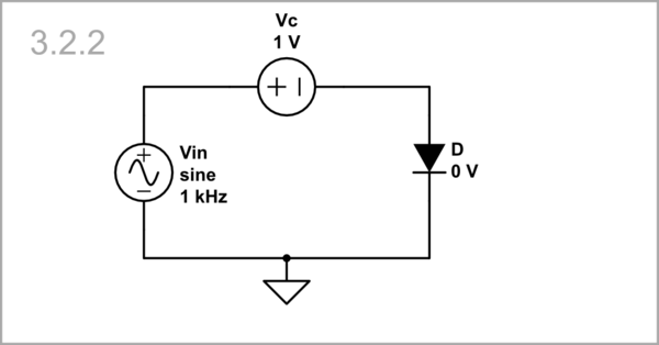
schematic

simulate this circuit

... so their voltages are added.
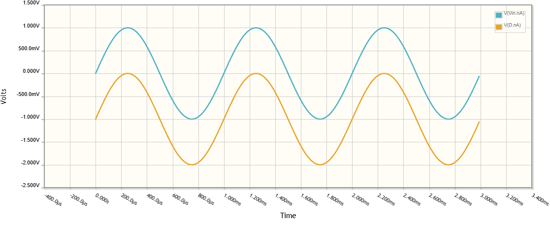
STEP 3.2.2

\$\endgroup\$

Your Answer

By clicking “Post Your Answer”, you agree to our terms of service and acknowledge you have read our privacy policy.

Not the answer you're looking for? Browse other questions tagged or ask your own question.