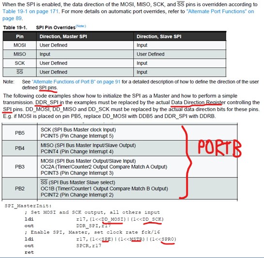
This is what I get, maybe slightly inaccurate, but the manual can explain best when you have the clue I am giving here.
It seems, looking at your code fragment, that to enable SPI, the register SPCR is written to.
SPCR should mean (Serial Peripheral [Interface] Control Register)
SPE should mean SP enable
MSTR should mean master
SPRO don't know
Once SPI is enabled, DDR_SPI overrides DDRB, it seems. So DDR_SPI has to be
set beforehand, as done in the code fragment.
SS negated is Slave Select. It is used when the SPI interface is programmed as a slave.
Yes. "1 << DD_MOSI" is the b3 in a byte. They use this to make MOSI (Master Out Slave In) an output,
along with SCK (clock), using DD_SCK.
#4 is correct, and they use this notation to make it clear that they are raising TWO bits (b3 & b5). But forget the numbers, use the mnemonics (DD_MOSI & alike). They could have used a mask, like you say (but your mask is wrong - too many "0" and one less "1"
6 & 7) Probably yes, but the manual clarify that much better than you or me.
- Left shifting because this is easy: you say bit 3, and you use "1 << 3" to create a mask for it. The other way would be possible: "0x80 >> 1" to indicate bit 6, but it looks horrible! Or you can use a mask "0b00001000" to define DD_MOSI (which I would prefer, like you), but you should stick to what the Atmel people did for us.
Don't worry too much... after you get aquainted with MCU hardware manuals, you will find that things are well explained and not too difficult to understand. You seem to know bits manipulation, and all boils down to that.
==== UPDATE after comment =====
The code fragment SPI_MasterInit cited in the question is a sort of pseudo code. I've found it at page 37 of the ATMega328P, and just above the example the manual states:
DDR_SPI in the examples must be replaced by the actual DDR register...
DD_MOSI, DD_MISO ... must be replaced ...
So, there is no register named DDR_SPI and no DD_MOSI and alike. One must set explicitly DDRB (in this case) doing something like
ldi r17, (1 << 3) | (1 << 5)    ; ...or equivalent...
out DDRB, r17
About using a pin as a simple I/O pin, yes - one must be sure that no peripheral using that pin is enabled. Maybe some peripheral can use that pin optionally, i.e. only if some particular feature is enabled. In this case, the SS pin works this way. The manual says that if the SPI peripheral is programmed as a Master, the SS pin is left alone (general purpose I/O) - but if the SPI peripheral is configured as Slave, the SS pin is forced to be an input.

