1
\$\begingroup\$

I'm making a pcb with a 4 layer stackup. The top layer and the bottom layer are used for signal and component routing. The 2 layer is GND (analog and digital planes) and the 3rd layer is Power (analog and digital planes too), like the image 1:

enter image description here

After this, I wanted to connect my pcb components with DGND (at the beginning of the design, all the ground plane is for the digital ground), so I made other via types, for each combination I wanted:

enter image description here

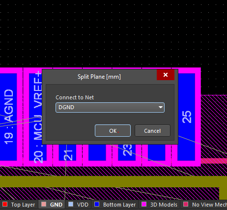
So, if I wanted to connect DGND with the components in the Bottom layer, I could use the Blind 2:4 via type. Then I did this. I connected the plane with the DGND net:

enter image description here

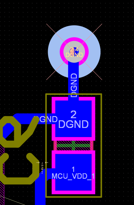
and then connected a decoupling capacitor to a 2:4 via:

enter image description here

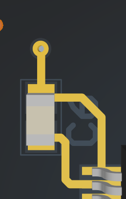
but as you can see, there is an X in the middle of the via, but the connection in this view and in the 3D view seems to be ok, so I don't understand what does it means. The 3D view is the following:

Bottom layer (4)

enter image description here

VDD plane(3) apparently no connected

enter image description here

GND plane (2), apparently connected

enter image description here

Top Layer (1) apparently no connected

enter image description here

I apreciate a lot if someone can tell me what's going on, or if its normal to see this X. I don't see any error message, but looking at other people projects in altium, the X doesn't appear at all.

\$\endgroup\$
8
  • \$\begingroup\$ As an advice, even if you are using those as plane, I always leave them signals to be able to work on them. For instance, if in some areas you need an analog ground, when you set it as a plane, you can't do it anymore. I don't think what you are seeing. If it is a DRC can you show us what rule is broken? To do it, you can run the DRC and in the report, it will be listed the error. \$\endgroup\$
    – Julien
    Aug 4 at 19:16
  • \$\begingroup\$ I agree, the only time to do a negative layer is with a solid ground layer. VDD is easier to route as a signal layer. Plus if you have to 'borrow' the layer to do crossover signals you can. \$\endgroup\$
    – Voltage Spike
    Aug 4 at 21:58
  • \$\begingroup\$ That's a pretty expensive type of via - it will significantly increase both the cost and lead time of your PCB. Is it not possible to use through hole vias, and just have it unconnected on layer 1? \$\endgroup\$
    – BeB00
    Aug 4 at 22:10
  • \$\begingroup\$ Actually, is this combination of vias even possible? Can they even do 1-3 and 2-4 together? \$\endgroup\$
    – BeB00
    Aug 4 at 22:13
  • \$\begingroup\$ For most boards, there is no need to use blind or buried vias. The PCB program will automatically ensure that a through via only connects to the required layers. \$\endgroup\$ Aug 4 at 23:43

1 Answer 1

1
\$\begingroup\$

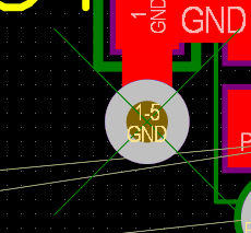
I see those on my altium when ground connects to an internal layer... but mine are green. They might be different colors due to the inner layer. Right click on the via and look for violations in the popup menu to see if you have any design rules it is not following.

enter image description here

\$\endgroup\$

Your Answer

By clicking “Post Your Answer”, you agree to our terms of service and acknowledge that you have read and understand our privacy policy and code of conduct.

Not the answer you're looking for? Browse other questions tagged or ask your own question.