0
\$\begingroup\$

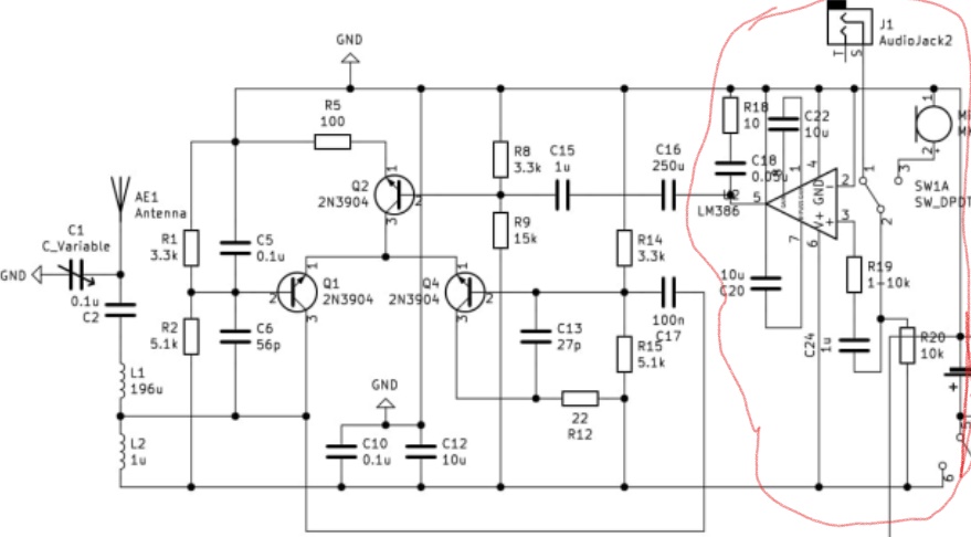
I have been trying to make an AM transmitter and I found this schematic from a persons college project. I understand what is circled in red but the rest I am struggling with. The part circled in red is in audio input and amplification. I also know that this project uses a Hartley oscillator to generate the carrier wave (535-1705 kHz) and that it uses one transistor for the amplitude modulation process. But I am very confused on how these work together and where they are on the circuit. His full project is on the link: https://web.mit.edu/6.101/www/s2020/projects/omotunde_Project_Final_Report.pdf

I would really appreciate if someone could highlight where the oscillator is and explain in this circuit, how amplitude modulation actually happens.

enter image description here

enter image description here

\$\endgroup\$
1
  • 5
    \$\begingroup\$ The schematics in that project report are designed for obfuscation, not understanding. It's bad enough (upside down antenna on the receiver and signal orientations on the pages) that I suspect it was intentional. If not, then the author remains highly confused and just managed to cobble this out and get it to work. \$\endgroup\$ Commented Aug 17, 2023 at 4:03

2 Answers 2

2
\$\begingroup\$

Calling the RF generator a "Hartley" is a stretch too far to bear.

I hope that stripping this oscillator/modulator to its bare bones, but maintaining its functional operation doesn't cause grief. I'm just too lazy to include every component. For example, biasing uses Thevenin equivalents.
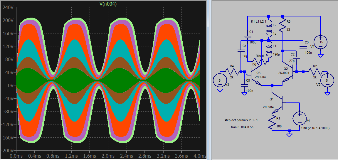
LTspice simulation 1kHz modulating MHz carrier
C3(100nf) provides positive feedback causing the two upper transistors to oscillate at the carrier frequency. Q1 varies audio-frequency current to the two upper oscillating transistors. Q1's collector current swings between 0 up to about 28mA at 1kHz here.
The purpose of C4(56pf) and C2(27pf) is unclear.

One might be careful of the oscillating tuned network (L1+L2, C1 and Rload). Without Rload, collector impedance of Q3 becomes so high that Q1 swings into a non-linear region where RF voltage swings below base voltage (near +5V). When Rload becomes high enough, the tuned network Q is reduced to the point where Q3 runs without base-collector forward bias at Q3. The plotted V(n004) monitors the node where Rload meets L1. This node is where the antenna is placed.
The antenna provides the necessary loading to keep Q3 from clipping. With no antenna Rload is small, amplitude becomes too high (light green plot where Rload=5 ohms). The transition point between clipping and proper operation in this simulation is where Rload>10 ohms roughly.


In my opinion, C2, C4, C5 and R3 are not necessary as primary functional parts. Their purpose may be to discourage oscillation at much higher frequency than desired... it is possible that this circuit could oscillate at 10's or 100's of MHz otherwise.

\$\endgroup\$
0
\$\begingroup\$

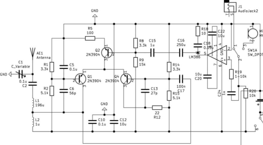
Q1 and Q4 are the oscillator. They’re a differential pair with Q2 modulating the tail current.

It’s a bit hard to see this because it’s been drawn upside down from the way it would usually be drawn, with ground at the top.

AM modulation happens because the gain of the oscillator is being changed, varying the amplitude of the signal.

\$\endgroup\$
1
  • 2
    \$\begingroup\$ The schematic is also drawn with the signal flow right to left, as opposed to the more easily understood left to right convention. \$\endgroup\$ Commented Aug 17, 2023 at 0:00

Your Answer

By clicking “Post Your Answer”, you agree to our terms of service and acknowledge you have read our privacy policy.

Not the answer you're looking for? Browse other questions tagged or ask your own question.