Yes, but not in a useful way.
Two basic reasons:
Loss is not, in general, proportional to these delays.
I assume you were thinking, let's take the triangular power dissipation waveform between I rise and V fall, and call that switching energy -- and wondered if there might be something about the other times too. I see that -- it's a good suspicion. Alas, it doesn't work out.
Actually, that method itself doesn't work out, which should be evident below, or I'll get around to explaining it.
There's switching loss in and around the event regardless, so, there being nonzero loss during these intervals, needn't really mean anything overall -- maybe it's a small percentage difference, a measurement error.
The better question to ask, then, is: is there significant loss here, in relation to the overall switching waveform? And, again, the answer is: yes, maybe, it depends.
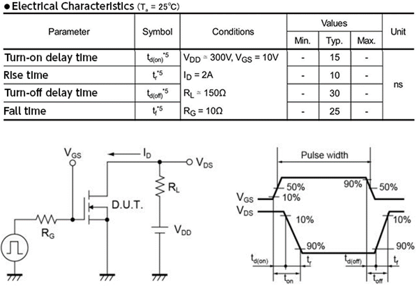
First, a few comments about the timing diagram: it's just that, a diagram. The relative timing of edges and 10/90% thresholds is arbitrary, shown only to label the respective intervals. It could equally well be that drain current flows for VGS < 10% and we get an apparent negative turn-on delay! This doesn't violate laws of causality in any way at all, it's simply a matter of definition -- poorly chosen definitions perhaps, but that's why we must not be too picky about such a simplified diagram, and more careful about what the actual conditions are.
In particular, the edges might or might not overlap, which is of paramount importance to the reactances in the circuit.

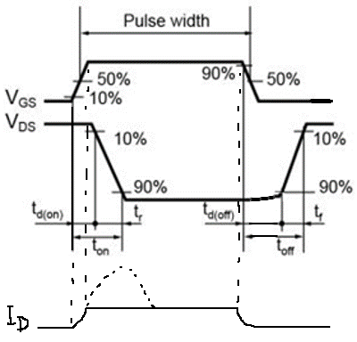
Here, I've modified the diagram to show things a little more realistically. I haven't changed the gate-rise timing, but just imagine it may overlap.
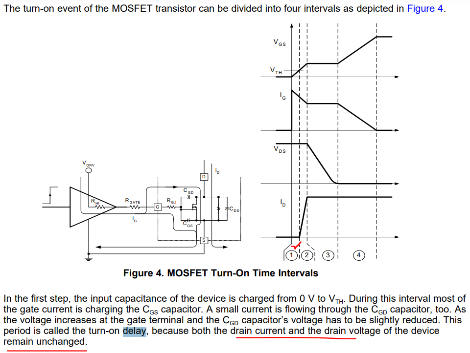
Assuming VGS is instantaneous (i.e., what we see at the pin is representative of what's on the transistor die itself), we see VDS initially high and VGS rise, so ID must also rise. This needn't yield an external current yet: first the drain self-capacitance must be discharged, for VDS to change, and only later does current flow through the resistor -- the test in question has a resistive load. (Other tests are done with constant-current or inductive loads, and may include a diode which causes hard-switching; check carefully for which type of test is being performed!) Thus, it can be that drain current (internally) rises quite a bit over the steady-state value, drawn as a dotted hump here.
Eventually, VDS falls, load current rises (again, resistor: load current goes as (VDD - VDS) / RL), and VDS settles into the resistive region. But even as voltage seems to have settled (below the 90% mark, say), current can still flow: Coss varies widely with VDS, and in particular can vary an extraordinary amount with some types, like Superjunction MOSFETs (which constitute almost all commonly available types above 300V or so) can have a ratio of Coss(0) / Coss(VDS(max)) over 100!
Now, during turn-on, RDS(on) is just so low that it will tend to short out Coss anyway (there are still internal charge-distribution effects in SJ types which take a little time to settle), but at turn-off, no such current excess is available, only ID driving the voltage up. And since capacitance at low VDS can be so extraordinary, this phase can take quite some time. In the process, drain current isn't really flowing -- ID is long since zeroed -- yet power nonetheless flows into the transistor. What's going on here? It's charging Coss, which takes energy, that's fine; but recall at turn-on, no complementary phase (capacitor discharge) occurred: energy goes into the superjunction, charging it, but it's discharged by the hard-switching turn-on, which costs turn-on energy.
So, this is one possible mechanism for energy to be lost during the delays, or around switching in general, that isn't simply the triangular waveforms commonly diagrammed -- which depends on how you're using the transistor, what the surrounding circuit and load are like, etc.
As it happens, the SJ energy loss effect is like a simple R+C in parallel with the transistor, so it has little loss at slow rates of change (100s ns, say), but incurs "full" switching loss when commutated rapidly (10s ns). Note this occurs regardless of "who" is doing the switching: you can strap such a MOSFET with gate to source, so it remains perfectly off, and run its VDS up and down and measure this loss mechanism independently.
For other types, again, it depends. The Coss ratio is large, easily more than 5, but there isn't necessarily loss associated with it (or at least as much as SJ). In hard switching turn-on, Coss energy (Eoss) is simply dissipated, no way about it; in ZVS resonant applications, this energy can be "stirred" with the load reactance, which requires a synchronized dance of proper switching/timing (but, as it happens, isn't terribly complicated, it largely reduces to variable-frequency drive), and obviously a specialized output network and other considerations, but this is, in short, why resonant converters are popular for compact, high efficiency power supplies.
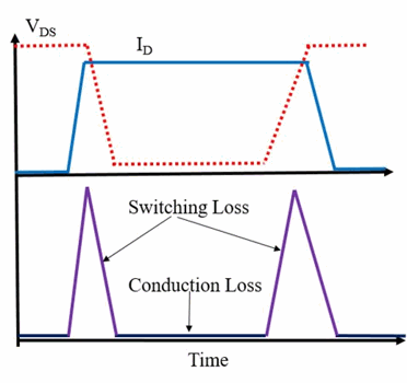
As for the triangle diagrams -- they are just that, diagrams. You'll see figures like this:

From: https://www.everythingpe.com/community/what-are-switching-losses-in-a-transistor
and, as we've now covered, all these slopes have weird curves to them instead -- ID(VGS) is a parabola (more or less), VDS drops sharply at high voltage, slowly at low -- and there can be other knock-on effects like the SJ internal resistance effect discussed above. In general, the power waveform will not be triangular, and this figure is at best a basic starting point; it is far from the final truth.
