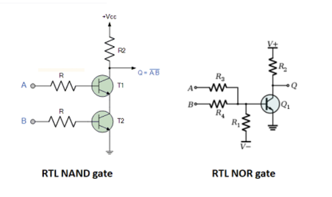
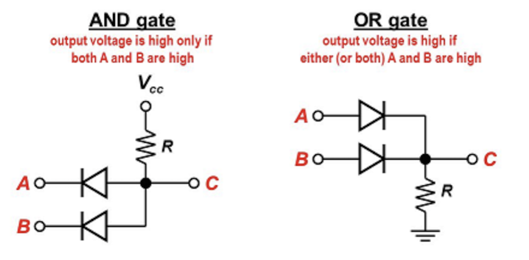
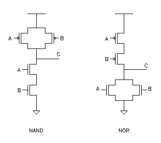
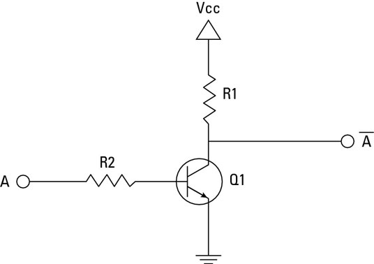
Does anyone know why image 3 has more transistors?
Yes.
Joking aside. The RTL and discrete diode-resistor circuits use resistors as pull-ups or pull-downs, which raise the current consumption. The CMOS circuit avoids this by switching off one of the driving sides.
Also, the basic advantage to using NAND or NOR gates in digital electronics?
There are no other simple gates in digital electronics. An inverter as such cannot operate on multiple input values. An AND or OR needs an additional inverter. A XOR is even more complex.
If you target the preference for NAND over NOR, the linked question already has the answer. There is no need for repetition.
- In the following image with diodes I'm assuming the voltage at C has two steps as current is applied to A and B. Please correct me if I'm wrong.
You are wrong, as the input signal is coded in voltage, not in current.
The discrete diode-resistor circuits assume that the driver on one input is strong enough to pull down (or up) its input to GND (or VCC) by its own. If both inputs are pulling, they may take different currents, but in sum the same.
For example, let's say VCC is \$5V\$, the forward voltage of one diode is \$0.7V\$, and the resistor is \$1k\Omega\$. If only one diode is conducting and pulling towards its rail, the current through the resistor is \$I_R = {5V - 0.7V \over 1k\Omega} = 4.3mA\$. The driving input needs to source or sink this current.
Now when both diodes are conducting, the corner case can have one diode with a clearly lower forward voltage. This one will source/sink all the current. In a theoretical ideal case both diodes have the same forward voltage, then each of them gets 50% of the current. The reality is somewhere in between.
- [...] There are NOT gates as circles, which adds even more transistors. Why the extra transistors?
Your assumption is wrong. The circles are NOT inverters by additional transistors. They mark the function of that transistor.
In regards to using NAND vs NOR, I see the following post which explains the advantage of NAND over NOR. It says NAND has less delay. I'm assuming it's because electrons pass the top transistors in parallel for NAND, however if you compare to NOR almost identical.
Your assumptions is wrong.
The answer explains that the delay depends on the relative size, which is smaller for the NAND.
It says NAND has less area, however looking at this example both appear to have same area.
Again, no. The sum of the relative numbers is 8 for the NAND and 10 for the NOR.
Also, in the resistor logic example NOR appears to have one less transistor and one additional resistor.
No. Both gates use 4 transistors each and no resistor.
The final comment is the NAND uses transistors of similar size. I'm unsure how that comment can be made from these images.
It can because the numbers at each transistor of the NAND are all "2". The NOR in contrast has 2 transistors with "4" and two transistors with "1".


