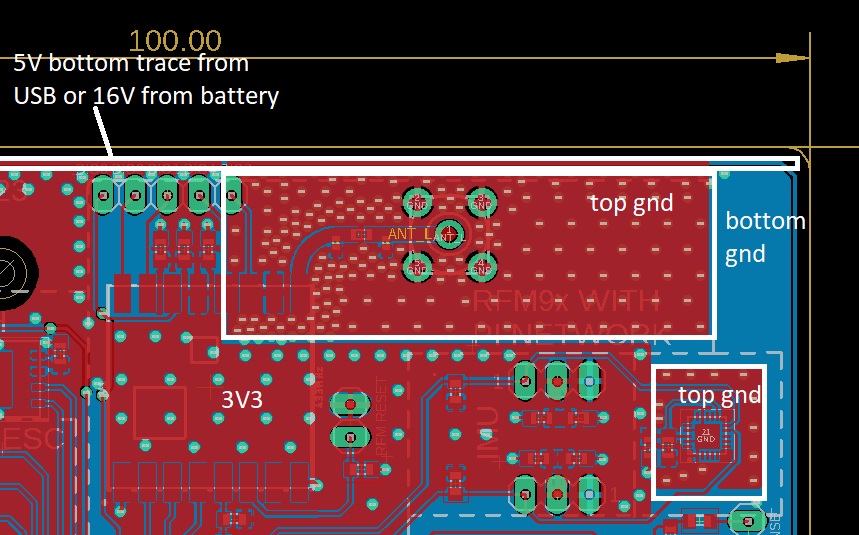
I have designed a custom PCB which among other things has an RFM69HCW (ignore the text on the PCB, it is wrong) capable of outputting +20dBm. The antenna connection is done using a PCB trace (42[mils] wide, 185[mils] first section, 240[mils] second section) with a PI network. This means that from the module pin to the SMA connector the trace is discontinued and was connected by a zero ohm resistor. The design was done using Eagle (free version) and thus I was limited to a board size of 100[mm]/3.93[in] by 80[mm]/3.14[in] and only 2 layers, with the bottom one being only GND. I did my best to keep the GND as solid as possible, with just 22 traces on the bottom and the longest trace being just 6[mm] and no discontinuation of the GND plane.
LE: Added schematic of the PI Network
Right now only a zero ohm resistor is populated in place of C16 on both boards. The PI capacitors (C15 and C17) are not populated and their values are not computed yet not even theoretically.
Also connected to the input of the RFM are three 603 MLCC capacitors rated 0.1uF@6V3, 1uF@6V3 and 10uF@6V3.
Now, I am no expert in RF engineering, and though I have experience in electronics and programming, RF is beyond my capabilities.
In my research prior to this design, I studied many of the online resources and I came across this document from Cypress/Infineon. At section 18.1 we read the following:
- Fill the unused area in the top and bottom layers with ground and connect it with the ground plane with many vias spaced not more than one-twentieth of the wavelength of the operating frequency.
- The bottom ground plane, together with the top ground plane and vias between the two ground planes, ensures that all traces are well shielded. This arrangement significantly improves the EMI and EMC performance.
Across my research, I came across this point again and again: Use vias to shield both the trace and the surrounding area so that they do not interfere with each other: as in RF signal does not go anywhere else but the antenna and the various signals from surrounding area do not impact the RF trace/signal. Thus I created a GND plane surrounding the RF trace, SMA connector, and part of the RFM module and placed many vias around the trace to shield/isolate it from the rest of the circuit.
Recently I learned that too many vias (like I have in this design) could potentially act as an antenna and radiate unwanted power in the surrounding area.
What I could not find anywhere was how many vias is too much and how many vias is not enough.
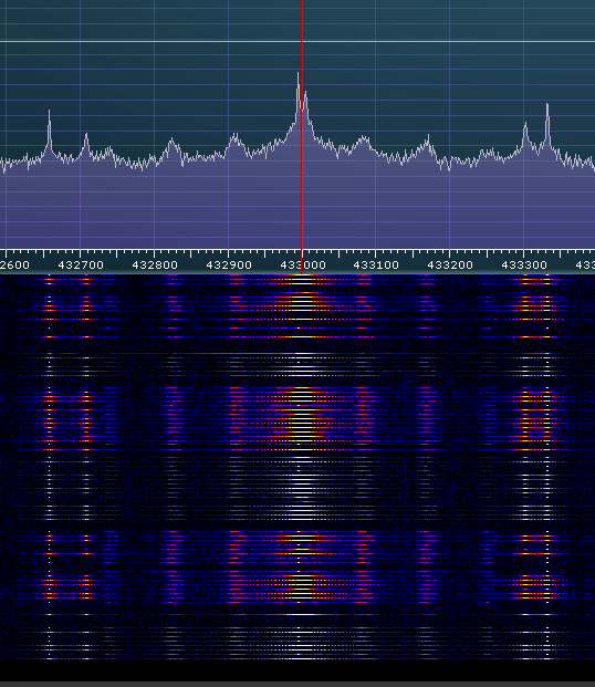
Now I have my two PCB's up and running with the first few packets being exchanged. What I am doing in the SW is setting up the Transmitter to blast packets at full power (+20dBm with Over Current Protection disabled - as stated in the datasheet). The Receiver (just a meter/three feet away) is receiving all packets with an average RSSI value of about -80dBm. I have an SDRUno nearby and while I do detect a lot of packets (there are still occasional packets not sent for unknown reasons yet) their RSSI appears to be in the range -80[dBm] to -90[dBm].
I will acquire a VNA in the next few days with the intent to measure both antenna impedance and RF source impedance and use the PI network to match the two if required.
My questions are:
- How many vias is too much?
- Do too many vias act as RF radiators rather than RF shields/isolators?
- Can some RF power go through those vias directly to GND plane thus losing effective RF radiated power at the antenna?
- Can the opposite be true at the receiver, as in RF power being absorbed by the vias and not enough RF signal being received by the receiver?
- Can I use a VNA (like NanoVNA) to measure these values, or at least to get a better idea of what happens in that part of the circuit?
LE2:
- Is it possible to use near-field probes to check RF power in that area? If so, are there any tutorials other than the official presentations from various manufacturers?
LE3: The antenna used is this one: ANT-433-CW-HWR-RPS. Datasheet states it is optimized for 433[MHz]


