2
\$\begingroup\$

This is a spin-off of the question I've asked before. I've received many interesting answers and summarized them there. I also accepted most interesting suggestion. During this time we also bought and tested two commercial devices, EM-A43 and LUGE-SR060 with external resistor. They work as expected but are expensive and have inconvenient (in our particular case, not in general) form factor.

So, I'd like to proceed with developing of our own device, and for this I need some help. I've selected two options from earlier discussion: comparator with MOSFET/IGBT and linear regulator with BJT. enter image description here

It is my understanding that the first circuit will work by rapid on/off switching, potentially creating a lot of noise. Also powering the comparator and gate driver from the very voltage being controlled might be problematic. On a plus side, the bulk of the dissipation will be on a resistor, with only switching losses on the FET.

The second circuit will control resistor current, keeping the voltage mostly constant. However selection of the resistor will be crucial, and the power dissipated on the transistor can be very high. I am planning on using MJH6284G with HS300-1R8-J or CJP400J1R8J.

I did preliminary calculations and stumbled upon an interesting phenomena. Let's say the circuit is designed to dissipate 450W. With 1.8R resistor it will dissipate 400W, the remaining 50W will be on transistor. However if the brakes applied gradually, the total power and current drop linearly, while the dissipation on the resistor drops squarely (due to 2 in I2R). For example 300W will be split 180/120 between resistor and transistor. This makes me worry of the second solution.

Requirements:

Total weight 230kg braking from 10km/h to full stop in 2s => 890J, 450W.
Voltage threshold 30V.

Questions:

  • Which circuit configuration is beter?
  • Are my calculations for power distribution between resistor and transistor correct?
  • How to power both circuits, considering the voltage fluctuations generated by circuits themselves?
  • Does the second circuit need biasing or bipolar supply and how can I implement it?

Clarifications:

The title refers to the control signal going into power stage. It is discrete on/off in case of comparator and linear when coming from differential amplifier.

It is important to notice that this circuit will only activate when the battery is fully charged AND the braking is hard or long. It can activate while driving down slope or hard braking right after disconnecting the charger, which may be never for any particular user. In all other cases the regen will simply be absorbed by the battery.

UPDATE

We have received additional info on the inner workings of the motor controller from the manufacturer. It turns out @MathKeepsMeBusy was spot on re charging pump involved in regen:

During regen the motor together with the associated bridge components create a boost converter. Since the motor has an inductance and together with the high and low-side FETs it becomes a boost converter SMPS, where turning on the low-side FET (high-side off) will cause the inductor in the motor to charge up and then turning on the high-side FET (low-side is off) the converter enters flyback mode and the current flows into the battery rail.

This does not change the question in any way, I just wanted to mention this interesting mechanism that turned my understanding of the process upside down.

\$\endgroup\$
29
  • \$\begingroup\$ Please explain what the voltage is that you wish to clamp and what series source impedance it has. Also mention what hold-up capacitance there is on the terminals marked \$\Phi\$. Both circuits are lacking values which, in my opinion means they are not really schematics in what I believe to be the true sense. Calculations might be useful but, simulations will always win the day in my opinion. Both circuits are linear and both look likely to be discrete. \$\endgroup\$
    – Andy aka
    Commented Oct 1, 2023 at 19:10
  • \$\begingroup\$ @Andyaka They are not actual schematics, they are concept drawings. The schematic is what I hope to end up with as a result of the feedback. The voltage threshold is 30V. I have no idea how to measure source impedance or capacitance. If you have suggestions I am all ears. Both are the complex combinations of battery, wiring, motors, bulk capacitors in motor driver, and quite a few additional electrical modules. \$\endgroup\$
    – Maple
    Commented Oct 1, 2023 at 19:24
  • \$\begingroup\$ @Maple you need to find out what the source impedance is (and bulk capacitance) or you have no way to calculate peak powers based on only knowing the full energy needed to be burnt. Your main question was which schematic is better (just saying). \$\endgroup\$
    – Andy aka
    Commented Oct 1, 2023 at 20:09
  • \$\begingroup\$ @Andyaka May I point out that manufacturers of the commercial regulators have no way of knowing this information, nor they include any limitations in datasheets. I've linked two of them in the beginning and two more in the original question. This leads me to believe that simple shunt regulator can be made to operate in wide range of the operating conditions. After all, its only purpose is to burn out excess power and keep voltage under threshold. Does it really matter where that power came from or how it was influenced by system inductance/capacitance? \$\endgroup\$
    – Maple
    Commented Oct 1, 2023 at 20:16
  • \$\begingroup\$ As I implied in my last comment, it's the peak power (the very short duration pulses of power that you might inadvertently take if you don't have a more complete picture of the full system) that is a certain MOSFET/BJT destroyer. And, it does totally depend on things you are unable to currently define. So, on that basis alone you have to use MOSFET on/off hysteresis and resistor power dissipation. That doesn't appear to be an option you have listed because both your circuits are linear in operation. \$\endgroup\$
    – Andy aka
    Commented Oct 1, 2023 at 20:43

2 Answers 2

1
\$\begingroup\$

A shunt regulator, whether digital or linear, works by dissipating power at the source, as much as in the series resistor. If the power supply is relatively "stiff", i.e., has a low source impedance, the shunt may burn out the power supply before voltage falls within the desired range.

A digital shunt regulator pulses the load, so that a series inductor could be inserted increase the source impedance and efficiency. A linear shunt regulator might find a use in some applications such as photovoltaic power, where input current is limited, or in very low-power circuits, where the waste is negligible.

So the big question is how this type of regulator will be used, and why you've chosen shunt regulation at all.

\$\endgroup\$
3
  • \$\begingroup\$ "So the big question is how this type of regulator will be used, and why you've chosen shunt regulation at all." The answers to these questions can be found in the original question here \$\endgroup\$
    – Maple
    Commented Oct 1, 2023 at 21:43
  • \$\begingroup\$ "If the power supply is relatively "stiff", i.e., has a low source impedance, the shunt may burn out the power supply before voltage falls within the desired range." Sorry, I am not good at analog circuits. Would not low source impedance mean that most of the power will be dissipated on a resistor, not on power supply? \$\endgroup\$
    – Maple
    Commented Oct 2, 2023 at 3:12
  • \$\begingroup\$ A resistor energy absorber could cost far less than the commercial units. Nichrome wire can be used to make 200W - 500W range air scpaced air cooled resistor. Or even many smaller ceramic air cooled are "cheap enough". Switch is not hard. Logic takes some design. \$\endgroup\$
    – Russell McMahon
    Commented Oct 4, 2023 at 1:51
0
\$\begingroup\$

Either can work. The switching implementation puts the energy in the R which is easier to specify and more rugged. But you have to tune and verify the switching behavior.

The linear approach requires an expensive transistor for the reasons you identified. And don’t just look at the front page of the data sheet. Check the thermals and the safe operating area curves - both fets and bjt’s have breakdown modes in their linear region.l characterized in the SOA curves. And note you can’t parallel fets in the linear region - you have to buy a big expensive one.

To power the circuit I think it’s wise to power from the rail being clamped and there is no problem with this. Use a linear regulator or a small shunt regulator with a zener.

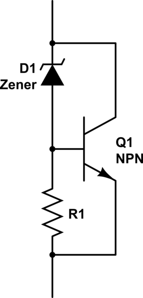
Note there is an even simpler topology for the linear solution. You can insert an R in this topology if you want and it can work with either BJT or fet (BJT has less Vbe variation but will burden the Zener with high current making it harder to specify).

enter image description herehttps://i.sstatic.net/L8PuI.png

\$\endgroup\$
1
  • \$\begingroup\$ Thank you for addressing the actual questions. It is good to know that it can be powered from actual rails being clamped with a simple linear regulator. The circuit you've suggested is a variant of Jasen's answer to the old question. The reason I've decided against it is that fine tuning it seems to be harder than simply adding variable pot to one input of a comparator/linear amplifier. \$\endgroup\$
    – Maple
    Commented Oct 1, 2023 at 22:37

Not the answer you're looking for? Browse other questions tagged or ask your own question.