2
\$\begingroup\$

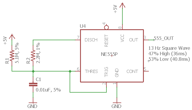
I was looking at a dead Molex "Suitcase" terminal applicators and found on its controller board this 555 circuit. It appears to be an astable multivibrator, but not the typical kind.

It lacks the reset pin being pulled high, or the typical 0.01uF capacitor on pin 5.

It also lacks a pullup resistor from pin 7 to VCC, but has a "pullup" on pin 6 to VCC.

I put the circuit on a breadboard and noticed I get a 13 Hz square wave with a 47/53 duty cycle, which is also odd, as on a vanilla astable multivibrator, the high time is typically larger than the low time, while here, the high time is lower than the low time.

How does this circuit work and why would someone do it this way?

555 Timer Circuit from a Molex Terminal Applicator from the 90's

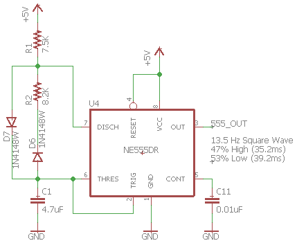
EDIT: Below was a circuit I breadboarded that got close, but doing it the way I am used to seeing it. 555 Timer, the normal way
\$\endgroup\$
2
  • 1
    \$\begingroup\$ The datasheet of an old NE555 or LM555 with a +5V supply shows its unloaded output going high to only +4.1V and to a low that is almost 0V. A Cmos 555 has an unloaded output that goes to each supply voltage and will produce a 50-50 squarewave. \$\endgroup\$
    – Audioguru
    Commented Oct 14, 2023 at 13:44
  • \$\begingroup\$ Does this answer your question? 555 astable resistor location \$\endgroup\$
    – Dave Tweed
    Commented Oct 14, 2023 at 21:03

2 Answers 2

1
\$\begingroup\$

The old bipolar 555 does not require /RESET tied to Vcc nor does it require a bypass capacitor on pin 5. It's recommended but not required.

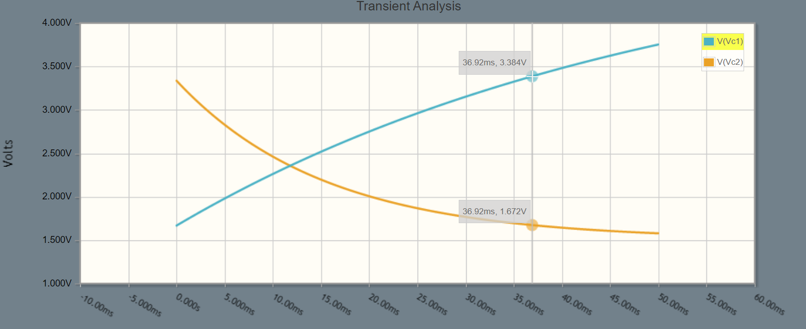
Rather than muck about with equations, let's be lazy and simulate the charge and discharge:

schematic

simulate this circuit – Schematic created using CircuitLab

enter image description here

Here I've ignored the currents flowing into or out of the trigger and threshold inputs and the leakage from the discharge terminal (as well as the saturation voltage of the discharge terminal).

We can see that the theoretical duty cycle is close to 50% and the frequency (with the simplifications) should be around 14Hz, which matches the observations well enough.

So you'd do it to get close to 50% duty cycle with the ancient bipolar 555, but I'm not a big fan of the circuit as described. I'd much rather a larger capacitor than 10nF and much lower value resistors and the circuit as shown has a lot of sensitivity to the ratio of the two timing resistors. It would not take much in the way of tolerances adding and 555 at the edges of guarantees have it not work at all. Maybe a mechanical designer fiddled with this on a breadboard until it sort-of worked..

\$\endgroup\$
0
0
\$\begingroup\$

Output high time - Capacitor charges between Vcc/3 and 2*Vcc/3 via R1. During this time the DISCH pin is high impedance and so no current flows through R2.

Output low time - DISCH pin is internally switched to approx 0 V and the capacitor discharges between 2*Vcc/3 and Vcc/3 via R2 but during this period R1 is still supplying some capacitor charging current which slows the discharge of the capacitor increasing the output low time to be slightly higher than the output high time. Close to a 50% duty cycle.

\$\endgroup\$

Your Answer

By clicking “Post Your Answer”, you agree to our terms of service and acknowledge you have read our privacy policy.

Not the answer you're looking for? Browse other questions tagged or ask your own question.