1
\$\begingroup\$

I'm trying to incorporate a ceramic chip antenna in a wearable device due to its low footprint and affordability. After reading the datasheet countless times and YouTube tutorials I'm still not 100% sure on how to make the perfect feedline.

I have used various impedance calculators and obtained the required values for track width and GND clearance, for a co-planar waveguide (this type of "trace" is suggested by the datasheet). My questions are:

  • Where does the RF feedline start at? The datasheet says it needs to have 50 Ohm. Does the impedance start counting right after the RF front-end pad up to the ceramic chip or from the pi-network circuit to the chip?

  • If the feedline comes from the RF front-end through a thin pad then a thin track is needed to connect to the thin pad. In this case, it will be way thinner than the feedline I computed. Through this approach, I obtained a track with at first 0.2mm (7.9 mil) and then it increases its width up to 1.06mm (41.7 mil; as computed for the 50 Ohm impedance). I'm not sure about this because I assume the thin portion has way higher impedance than the thicker portion that was computed for 50 Ohm. Won't this wdith transition add up (like resistors in series) to the overall feedline resistance?

  • If the previous point is true, I had the idea of, instead, computing the feedline parameters by fixing the variables Impedance = 50 Ohm and Track Width = 0.2 mm (so has to prevent width changes), but then it results in a required clearance of 0.07 mm (2.8 mil) which seems to be too low for most manufacturer.

How would you explain / solve this? Should I just go with my current design and hope it works?

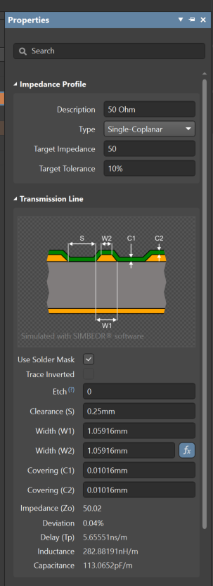
Computed parameters for co-planar feedline

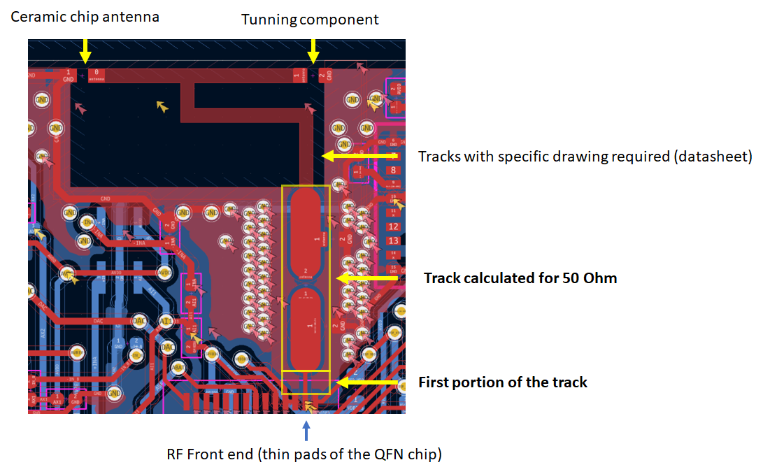
Antenna traces + co-planar feedline

Thanks!!

EDIT:

After checking everything mentioned, I would just like to know if the transition to the "antenna region" will be problematic (i.e. will it lead to wave reflections?) on the last picture.

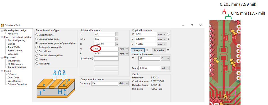
Updated feedline parameters:

Updated feedline parameters

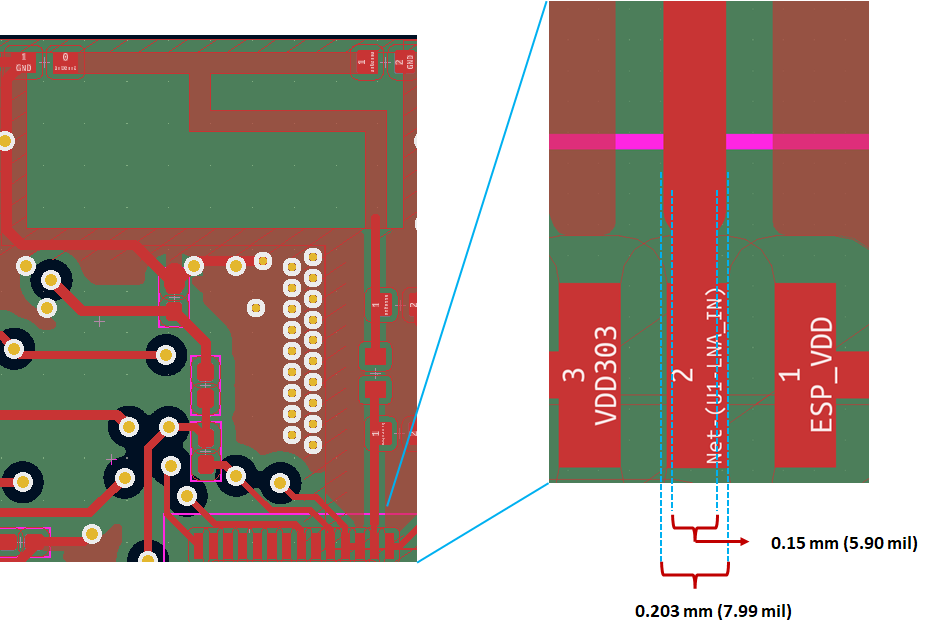
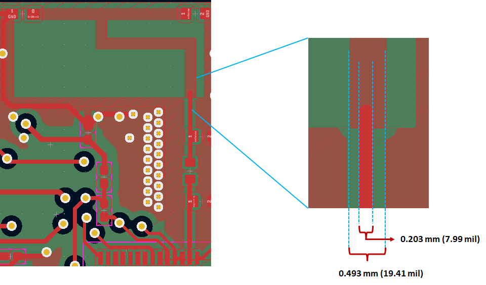
Width transition from RF front end to antenna feedline (way better now):

Width transition from RF front end to antenna feedline

Width transition from antenna feedline to "antenna region" (it still feels like a big transition, so this is where I'm not sure whether it's OK):

Width transition from antenna feedline to "antenna region"

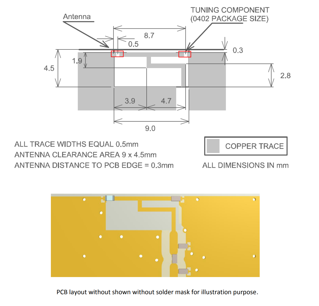
Antenna's datasheet (they also seem to have a non-negligible width transition):

enter image description here

\$\endgroup\$
14
  • \$\begingroup\$ Consider the board thickness. Make this a four-layer board and all your troubles will disappear, most likely. \$\endgroup\$
    – Hearth
    Commented Oct 20, 2023 at 20:37
  • \$\begingroup\$ @Hearth I'm sorry but I don't see how increasing the number of layers would solve my specific problem. The board thickness is 1.2 mm (47.2 mil) which was considered in the calculations \$\endgroup\$ Commented Oct 20, 2023 at 20:40
  • 1
    \$\begingroup\$ You forgot to mention operating frequency and lengths of tracks that are not 50 ohm. \$\endgroup\$
    – Andy aka
    Commented Oct 20, 2023 at 20:50
  • 2
    \$\begingroup\$ @AfonsoFerreira no, it's not the same! As Hearth explained, if you have 4 copper layers instead of 2 in a board, then the next layer from the top layer is closer. And that changes the geometry of your 50Ω traces for the smaller, and the signal properties for the better. And, you say, the bottom is "practically" a ground plane: that won't do! it needs to be a continuous ground plane (or very low impedance ground referenced). In any case, you must not have any gaps in that plane – and you're literally running a trace through that, so that's where you build a mismatch and an unintended slot… \$\endgroup\$ Commented Oct 20, 2023 at 21:27
  • 2
    \$\begingroup\$ Device operation alone is hopeless without a solid ground plane underneath it; surrounding components are spaghetti flapping in the wind around the coat-hanger antenna. A solid ground plane is required to support the antenna and keep transmissions out of your surrounding circuit. \$\endgroup\$ Commented Oct 20, 2023 at 21:27

1 Answer 1

0
\$\begingroup\$

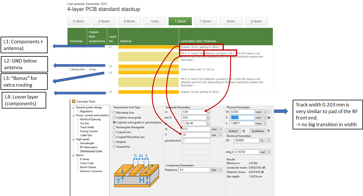
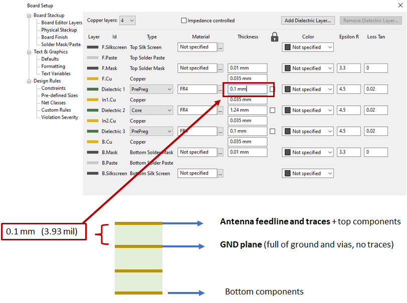
Thank you for the help guys. I have updated the design. Apparently, as you suggested, switching from 2 to 4 layers, allow to make the H parameter (thickness in the co-planar waveguide w/ GND plane) considerably smaller simply because, whilst the original total PCB thickness is maintained, the GND plane is now closer to the upper layer (0.1 mm instead of 1.2 mm / 3.93 mil instead of 47.24 mil). Consequently, this influences the calculus of the other feedline parameters (W and S), allowing to use thinner tracks and maintaining the 50 Ohm target impedance.

I have attached images of the resulting changes.

Calculus of new feedline parameters

Resulting feedline in PCB (upper layer)

1st (upper) and 2nd layer (GND plane)

\$\endgroup\$
1
  • \$\begingroup\$ Double check the dielectric constant of your manufacturer's prepreg too. It varies a lot. (so much, in fact, that you'll need to be able to accept significant variations from the quoted number, too--but it's not going to kill anyone if it's 45 Ω instead of 50.) \$\endgroup\$
    – Hearth
    Commented Oct 23, 2023 at 11:35

Your Answer

By clicking “Post Your Answer”, you agree to our terms of service and acknowledge you have read our privacy policy.

Not the answer you're looking for? Browse other questions tagged or ask your own question.