1
\$\begingroup\$

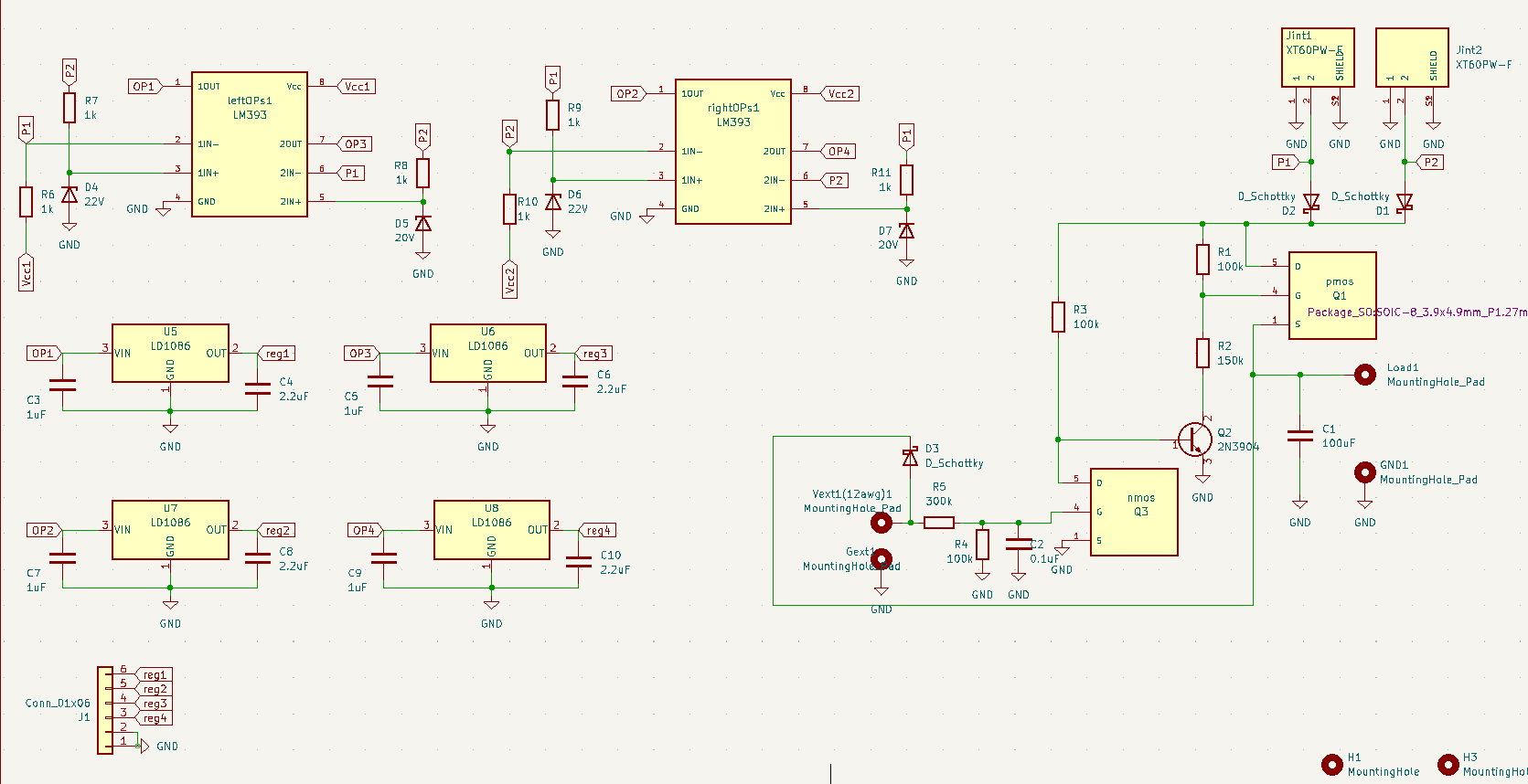
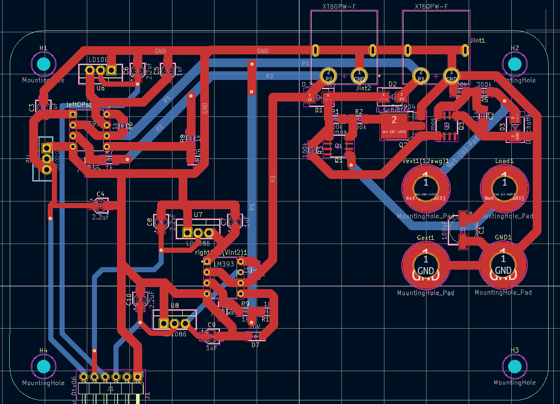
I have designed the PCB below and would like some advice on good practice for my PCB routing / board schematic. Are there any design considerations that I should be paying attention to for the design?

This is a power switching board that is designed to handle 30 VDC @ 5 A. It uses transistors for switching, and comparators for measuring the voltage difference between two batteries. I've used thick traces, but I'm slightly concerned that their close proximity to each other may induce interference.

Please let me know if there's any other information needed and I can provide it.

enter image description here

enter image description here

\$\endgroup\$
22
  • 2
    \$\begingroup\$ A ground plane is one of those good practices = you can skip that part of the routing. There's more reading from other questions here at EE, like this one: electronics.stackexchange.com/questions/539064/… \$\endgroup\$
    – MiNiMe
    Commented Nov 15, 2023 at 6:04
  • \$\begingroup\$ You have big traces that switch layers with a single via. You can look up via current capacities given the dimensions but they also add inductance which might be a problem depending on the frequencies involved. I suggest either adding more vias or rerouting to make them unnecessary. \$\endgroup\$
    – vir
    Commented Nov 15, 2023 at 6:25
  • 3
    \$\begingroup\$ Maybe.. My feeling is that before even thinking about routing, your placing looks not good. Good placing for a switcher means that it is much tighter and that you need hardly any long traces. Then again before even thinking about placing, one would need a good schematic. This is not one for me. It looks straight away incomprehensible to me. So I suggest you begin with making a good schematic, then understand placing. Routing is the easiest part of these three things to learn. \$\endgroup\$
    – tobalt
    Commented Nov 15, 2023 at 6:56
  • 1
    \$\begingroup\$ @makotoyuki a ground plane is what you should concentrate on fixing first. Fix that then show the new layout. With GPs, track length becomes nearly irrelevant to induction problems <-- I think you haven't grasped this yet have you? \$\endgroup\$
    – Andy aka
    Commented Nov 15, 2023 at 8:50
  • 2
    \$\begingroup\$ Source and drain of Q1 are swapped, all pads of Q1 should be used for heat spreading, LM393 has open collector outputs, so U5 - U8 never receive a signal. Common mode input voltage range of LM393 is violated, input above supply. P1 and P2 need a resistor to GND to define a voltage if nothing is plugged in. \$\endgroup\$
    – Jens
    Commented Nov 16, 2023 at 21:57

2 Answers 2

3
\$\begingroup\$
  • A common ground plane is always recommended.
  • Use copper pour to make the ground plane available everywhere possible
  • use a trace width calculator to ensure that the traces can carry the required current. (this software is a good free offline calculator for various PCB-related calculations : https://saturnpcb.com/saturn-pcb-toolkit/)
  • Triplet routing will be helpful for close-proximity routing of traces (https://www.edn.com/design-pcbs-for-emi-part-3-partitioning-and-routing/)
  • A minimum of 0.25mm PCB edge clearance is needed for manufacturing. check with your manufacturer.

If you have specific questions, put them in the comments.

\$\endgroup\$
1
\$\begingroup\$

I can tell what I know:

  • calculate trace width, use more with some margin and excess for power ones
    ** switching nodes need thicker traces to avoid parasitic inductance and elements must be close to avoid parasitics
  • Important is to use the rule of thumb for the gap between HV traces, not sure about the value and I will not post it for safety reasons and responsibility concern
  • watch for parasitic capacitances too (i feel this is less important in most cases)

In other words, when you design layout you should focus on parasitics and responsibility, safety

Divided in groups, I get:

responsibility:

  • the gap between HV traces
  • the trace width

    parasitics:
  • trace inductance
  • capacitance between traces
  • differential pairs for diff signals
  • impedance matched and terminated transmission lines for cables
  • use polygon unless application needs to not use

    I dont know if i know everything but at least this is a good starting point for beginner, I succeeded to make some good boards using these. One of them was a complex system with HV and different communications and linux system on module and all worked. I had issues only with the ethernet but it wasnt the layout.

When you have IC for example, you can use a short thin trace from a pin to longer thick trace, this is common practice

Recently I found a good article about this, you can search for example "boost converter layout" There are many good pdfs from manufacturers there

They are many things in layout design, I cant remember everything at the moment and missed some.

Sometimes good to use vias, some times bad Your learn flow will tell you piece by piece, I told you the basics of safety first and performance sweetness

\$\endgroup\$

Your Answer

By clicking “Post Your Answer”, you agree to our terms of service and acknowledge you have read our privacy policy.

Not the answer you're looking for? Browse other questions tagged or ask your own question.