2
\$\begingroup\$

I would be very happy if anyone can help me find answer regarding to questions below:

The lead compensator is added to the system to increase the phase margin.

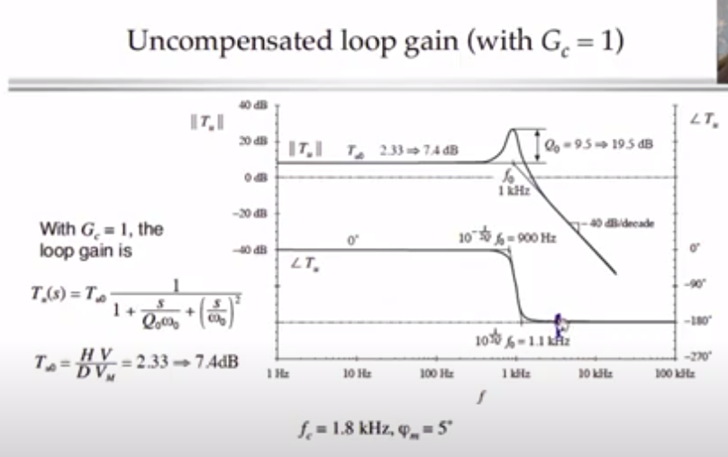
1'st picture is related to the uncompensated loop gain-phase graph.
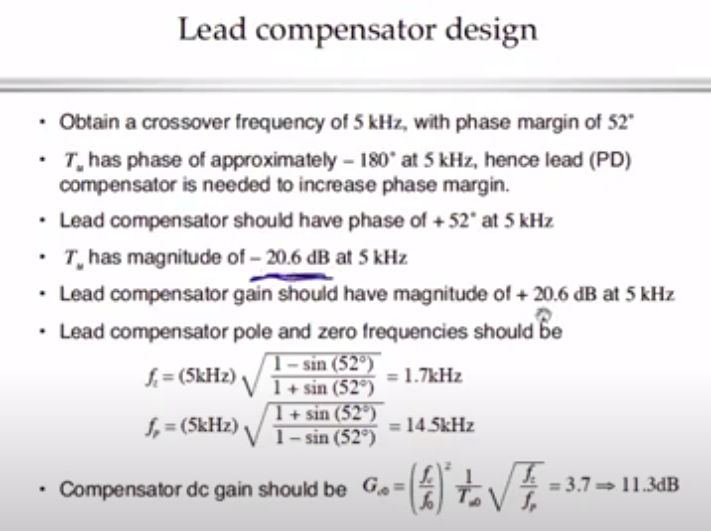
2'nd picture is the summary of the lead compensator. Poles and zeros are calculated to be added to our uncompensated transfer function.
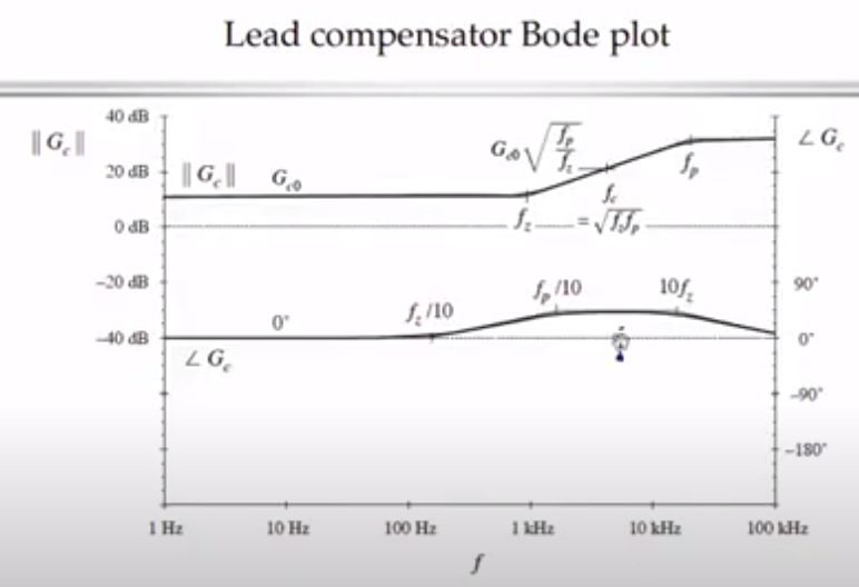
3'rd picture is the bode plot of lead compensator calculated to be added to the system.

My question is how did they calculate the compensator dc gain stated at the bottom of the 2'nd picture as Gc0= (fc/fo)*2x(1/Tco)x sqrt(fz/fp). I could not undestand that.

enter image description here

Source : Indus Electric Offical - Power Electronic 3 4 6 Design Example - https://www.youtube.com/watch?v=ABY43mX7UQo

enter image description here

Source : Indus Electric Offical - Power Electronic 3 4 6 Design Example - https://www.youtube.com/watch?v=ABY43mX7UQo
enter image description here

Source : Indus Electric Offical - Power Electronic 3 4 6 Design Example - https://www.youtube.com/watch?v=ABY43mX7UQo
\$\endgroup\$

1 Answer 1

4
\$\begingroup\$

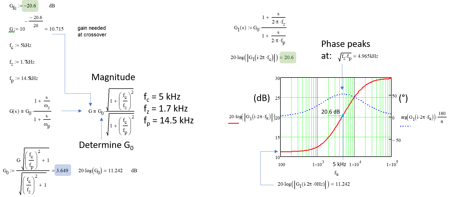
You need to design your active filter - the compensator - so that it exhibits a gain of 20.6 dB at 5 kHz. Calculate the magnitude of the filter with the selected pole-zero pair. This pair is positioned to meet the targeted phase boost:

\$|G(f_c)|=G_0\frac{\sqrt{1+(\frac{f_c}{f_z})^2}}{\sqrt{1+(\frac{f_c}{f_p})^2}}\$.

You know that this magnitude should compensate for the 20.6-dB attenuation at 5 kHz. Knowing the pole and zero selected for boosting the phase by 52°, what should \$G_0\$ be so that \$|G(5\;\mathrm{kHz)}|=20.6\;\mathrm{dB}\$:

enter image description here

You can also have a look at my free 90+ ready-made templates running on the demo of SIMPLIS for most of them. There are plenty of converters with an automated compensation procedure and the buck in VM and CM is there.

The expression used by Pr. Erickson in the 2nd picture, considers the high-frequency response asymptotes of the power stage \$H\$ and the compensator \$G\$. We know that the loop gain magnitude \$|T|\$ must be equal to one (or 0 dB) at the selected crossover frequency \$f_c=5\;\mathrm{kHz}\$.

The power stage transfer function is \$H(s)=H_0\frac{1}{1+\frac{s}{Q\omega_0}+(\frac{s}{\omega_0})^2}\$. If you consider that the crossover frequency is after the resonance \$f_0\$ - which is the case for proper compensation of a VM buck converter - then, you can write \$H(s)\approx H_0\frac{1}{(\frac{s}{\omega_0})^2}\$. In magnitude, you thus have \$|H(f_c)| \approx H_0(\frac{f_0}{f_c})^2\$.

Same goes with the compensator: \$|G(f_c)|\approx G_0\frac{\sqrt{(\frac{f_c}{f_z})^2}}{\sqrt{(\frac{f_c}{f_p})^2}}\approx G_0 \sqrt{\frac{f_p}{f_z}}\$. Now, if you write the complete loop gain magnitude observed at crossover, you have: \$(\frac{f_0}{f_c})^2H_0\sqrt{\frac{f_p}{f_z}}G_0=1\$. Solving for \$G_0\$ which is the dc gain of the compensator, you have \$G_0=(\frac{f_c}{f_0})^2\frac{1}{H_0}\sqrt{\frac{f_z}{f_p}}=3.67\$.

\$\endgroup\$
4
  • \$\begingroup\$ Thank you sir for your nice explanation. I understood your way of explanation but do you have any suggestion how to express it as in the 2'nd picture ? how did they come up with different kind of expression ? @Verbal Kint \$\endgroup\$
    – Mhan
    Commented Dec 4, 2023 at 13:37
  • \$\begingroup\$ @Mhan, I added the explanation for the expression. I prefer using the complete expression, it does not really complicate things and there is no ambiguity then. \$\endgroup\$ Commented Dec 4, 2023 at 14:48
  • \$\begingroup\$ Thank you so much sir for your nice explanations. @Verbal Kint \$\endgroup\$
    – Mhan
    Commented Dec 4, 2023 at 15:41
  • \$\begingroup\$ Glad if I did shed some light on this issue! \$\endgroup\$ Commented Dec 4, 2023 at 15:44

Your Answer

By clicking “Post Your Answer”, you agree to our terms of service and acknowledge you have read our privacy policy.

Not the answer you're looking for? Browse other questions tagged or ask your own question.