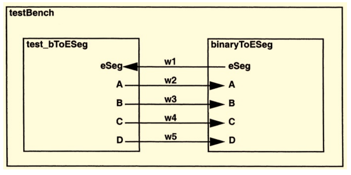
I am a beginner in Verilog, and when I study the testbench file, I am very confused about how the wires behave between the submodules in the file.
The testbench file:
module testBench;
  wire w1, w2, w3, w4, w5;
  binaryToESeg d (w1, w2, w3, w4, w5);
  test_bToESeg t (w1, w2, w3, w4, w5);
endmodule

module binaryToESeg
  (input A, B, C, D,
   output eSeg);
  nand #1
    g1 (p1, C, ~D),
    g2 (p2, A, B),
    g3 (p3, ~B, ~D),
    g4 (p4, A, C),
    g5 (eSeg, p1, p2, p3, p4);
endmodule

module test_bToESeg
  (output reg A, B, C, D,
   input eSeg);
  initial // two slashes introduce a single line comment
    begin
    $monitor($time,,
      "A = %b B = %b C = %b D = %b, eSeg = %b",
      A, B, C, D, eSeg);
    //waveform for simulating the nand ftip ftop
    #10 A = 0; B = 0; C = 0; D = 0;
    #10 D = 1;
    #10 C = 1; D = 0;
    #10 $finish;
  end
endmodule
The image provided by the book:
Above is the image provided by the book illustrating the interconnection of Design and Test modules. However, from the code to instantiate the two modules named d and t, I find that there is no reason for w2 to connect port A between these two modules.
Besides, why is the w2 pointed to the right instead of pointing to the left and w1 pointing to the left instead of pointing to the right? How can I define the direction of w2 and the remaining wires?
I think the Verilog code here adheres to IEEE Std. 1364-2001.

