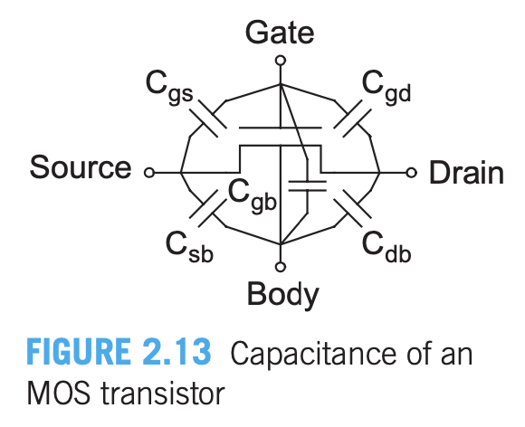
A MOSFET is, in reality, a four-terminal device with capacitances between each pair of terminals:
These capacitances are, of course, the standard MOSFET intrinsic and extrinsic differential capacitances (i.e. they are defined as \$C = dQ/dV \$ where \$Q\$ is the charge on one of the terminals and \$V\$ is the voltage difference between said terminal and the other terminal).
That being said, it is well known that when we do digital design, we sweep a lot of this under the rug. Indeed, in their CMOS VLSI Design, Weste and Harris claim that
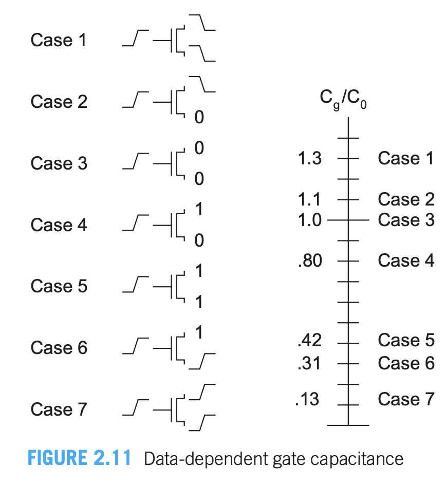
(1) It is convenient to view the gate capacitance as a single-terminal capacitor attached to the gate (with the other side not switching [this is in turn equivalent to saying that the capacitance's other node is ground, as discussed here]). (2) Because the source and drain actually form second terminals, the effective gate capacitance varies with the switching activity of the source and drain. Figure 2.11 shows the effective gate capacitance in a 0.35 um process for seven different combinations of source and drain behavior [Bailey98].
Figure 2.11 is from the Bailey paper (D. Bailey and B. Benschneider, “Clocking design and analysis for a 600-MHz Alpha microprocessor,” JSSC, vol. 33, no. 11, Nov. 1998, pp. 1627–1633) and is provided below:
Even after reading the Bailey paper and the sources cited therein, I am still not sure I understand the nature of the approximations being made. I think it is fair to say that there are two approximations being made though. I am thus led to the following two questions. As an example to illustrate, I will imagine an inverter switching to 0 on its input (1 on its output, though this isn't relevant for the question on the gate here) and focus on the NMOS transistor therein.
(1) The first approximation, I believe, is that with respect to the Gate node (i.e. if there is some circuit driving this node) then we can delete the capacitances \$C_{gs}, C_{gd}\$ and then there is some equivalent capacitance \$C_g\$ which we can put between the Gate node and ground such that, for a given stimulus from the driving circuit to our inverter, the delay until the Gate node charges and discharges is the same as it otherwise would be if we hadn't made this approximation. My question is whether this understanding is correct (i.e. is it the correct understanding of Weste and Harris's comment I have labelled (1) above) and, if so, how we justify this? Also, is it fair to say that this "equivalence" is only in the sense of producing the correct delay for the Gate, but not that it will have the exact same temporal dynamics (e.g. the rise time may differ even if the delay is the same).
(2) The second approximation, I believe, is that we can use the MOS differential capacitances to determine this delay. Given that the relevant charge-storage elements are nonlinear, I suppose a strictly rigorous argument for the time it would take to discharge the gate is the time \$t_d\$ at
$$I_{out}(V_g(t)) = \frac{dQ_{gs}(V_{gs}(t))}{dt} + \frac{dQ_{gd}(V_{gd}(t))}{dt} = \frac{dQ_{gs}}{dV_{gs}}\frac{dV_{gs}}{dt} + \frac{dQ_{gd}}{dV_{gd}}\frac{dV_{gd}}{dt}$$ $$ \equiv C_{gs}\frac{dV_{gs}}{dt} + C_{gd}\frac{dV_{gd}}{dt}$$ where \$I_{out}\$ would is some function of the gate voltage on our inverter depending on the nature of the PDN in the driving circuit. We see that we have reduced the problem to the form involving these nonlinear differential capacitances. This is a differential equation for \$V_g\$ (uncoupled if \$V_s,V_d\$ are constant, though that wouldn't be the case in our inverter. The "data-dependence" noted in Fig 2.11 comes, I assume, from the dependence on \$V_s\$ and \$V_d\$?). Is this basically how one uses the nonlinear differential capacitances of a MOSFET to calculate delay and other times of interest?
If there are any sources that really carefully analyze the approximations which get made here, it would be more than enough to point me to that. Sorry if this question is unfocused. I've tried to spend a lot of time thinking about it but there really does seem to be a lot going on with device modelling here, and in digital design texts it's really swept under the rug. In the end I'm just looking to understand "in principle" what's going on. Thank you!


