1
\$\begingroup\$

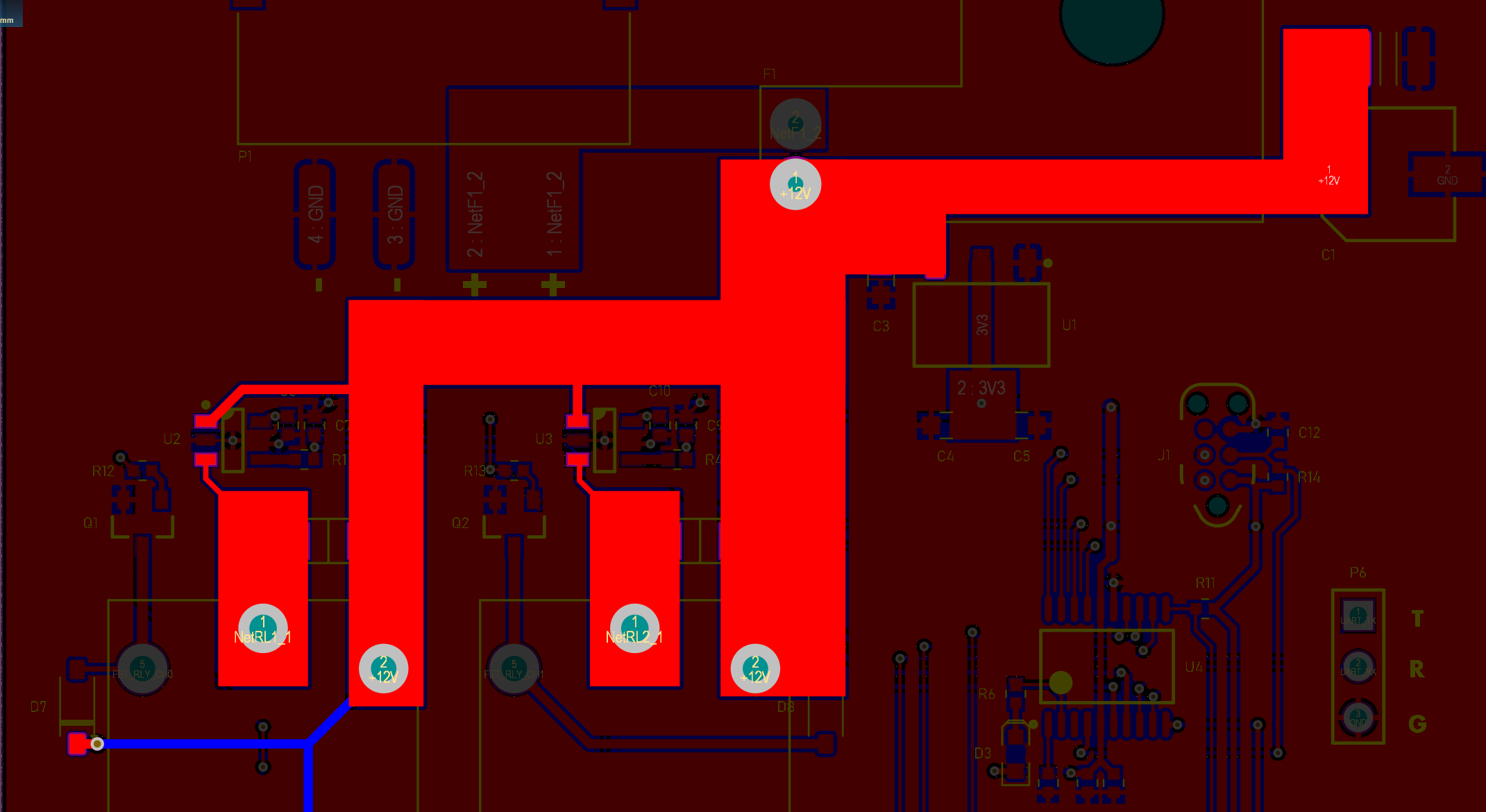
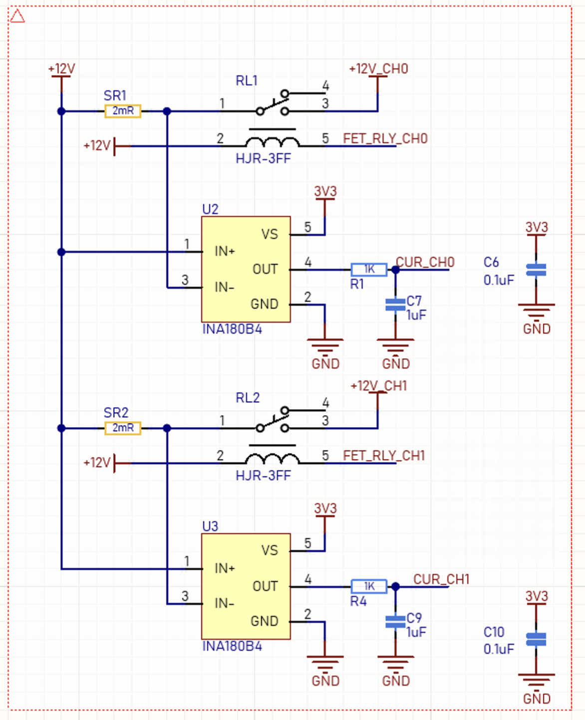
I've designed a two-channel current sensing circuit integrated into a board that outputs two separate signals. However, I'm encountering an issue where one channel seems to influence the other, which, to my understanding, should not happen.

Each channel in this circuit has its own current sensing component, but it appears that the operation of one channel is affecting the other. Additionally, I've observed that when there is no load connected to either channel, the circuit functions correctly. However, under load, the behavior changes.

Specifically, when a 5 A load is applied to only one channel, the voltage readings are as expected, but when one channel has a 5 A load and the other has a 1 A load, the voltage readings across the channels are not as expected. This discrepancy in voltage readings under different load conditions is puzzling.

I'm trying to figure out the root cause of this problem and understand why the voltage readings are affected in this way. Could this be a result of some form of interference, a design flaw in the circuit, or something else?

Furthermore, if there is a consistent relationship between the interactions of these two channels, I would like to know what formulas or calculations can be applied to predict or compensate for this influence.

Any insights or suggestions on how to diagnose and resolve this issue would be greatly appreciated.

enter image description here enter image description here

\$\endgroup\$
2
  • 1
    \$\begingroup\$ What does "not as expected" mean? Show us pictures of the board and the test setup. \$\endgroup\$
    – vir
    Commented Jan 16 at 0:21
  • \$\begingroup\$ Looks like both channels feed from the same supply (+12V). Don't forget the internal resistance of the supply. At 5A, this could be significant. Explaining the intended operation in detail would also be helpful. Whatever is down the line (at +12V_CH0 and *_Ch1) could be significant too. Also, what is your PCB design here? You could have coupling between the two channels, although this doesn't at first seem to be the issue (1A cross coupling at 5A would be quite a lot) \$\endgroup\$
    – DELTA12
    Commented Jan 16 at 0:21

2 Answers 2

2
\$\begingroup\$

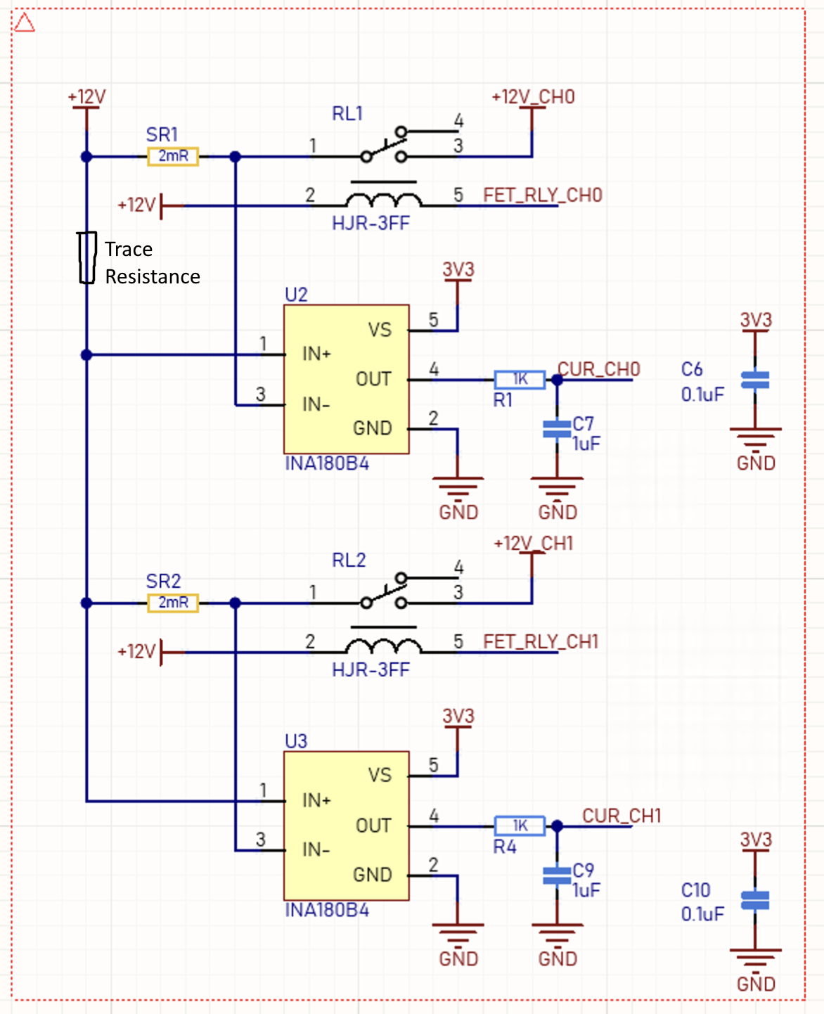
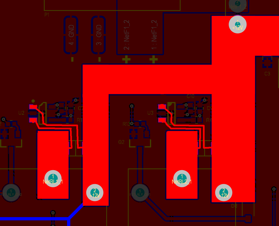
If the layout follows the schematic, current going to the output on the bottom creates a voltage drop on the trace resistance, which will be measured by U2.

enter image description here

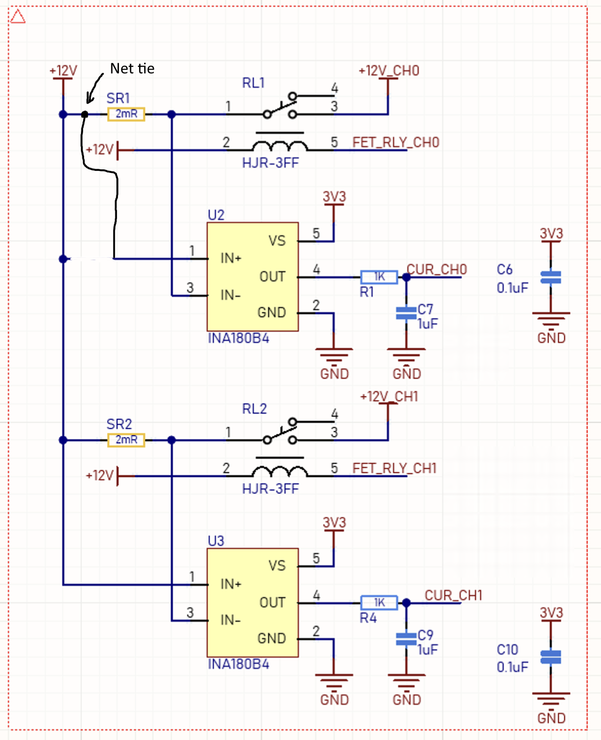
It should be routed like this instead, preferably with a note on the schematic.

enter image description here

If U2 is some distance away from SR1, then the two sense lines should be routed as a differential pair. To have the design rule check enforce it, you can put a net tie which makes the two sense lines into different nets from the power traces. This is especially useful if the power traces are copper pours, to prevent the sense lines from being connected to the wrong place.

Layout around the sense resistor is important for accuracy too.

EDIT:

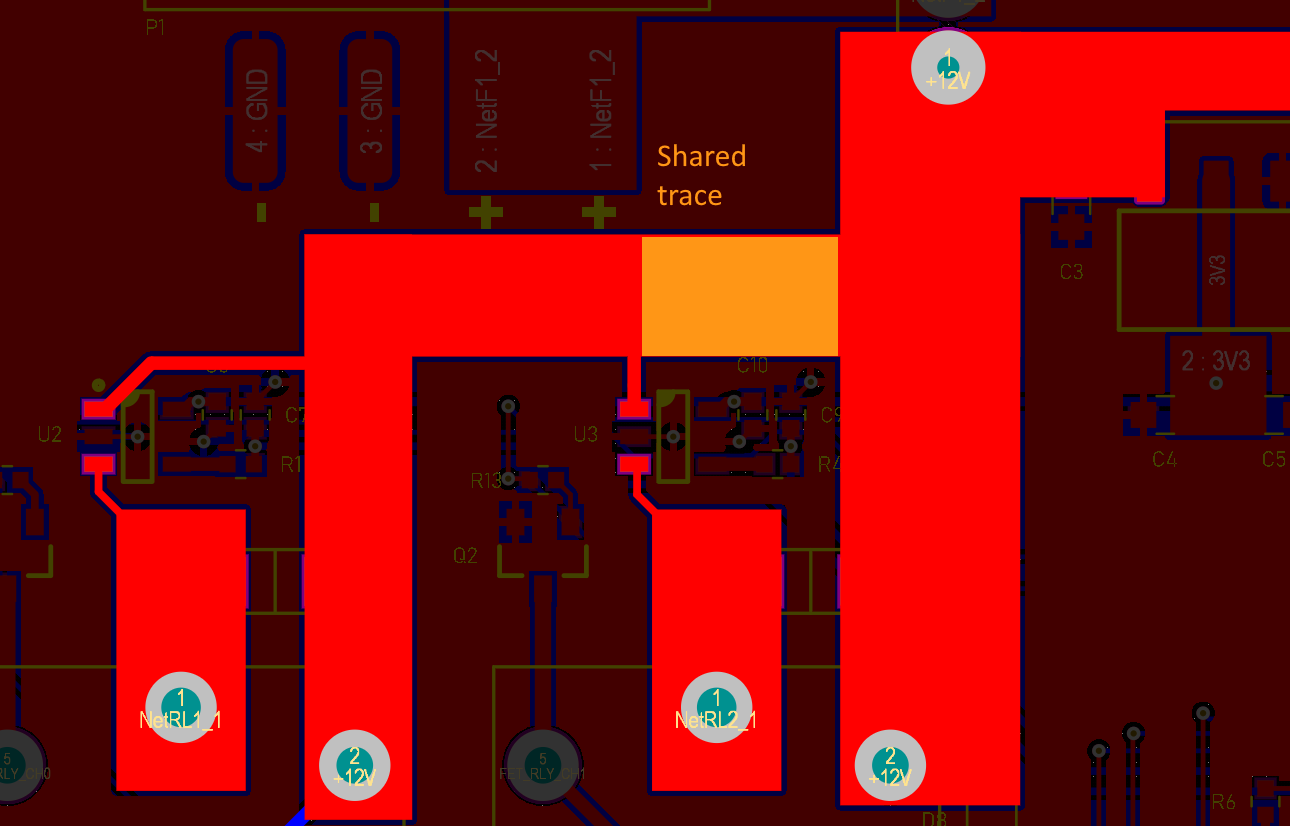
It would be useful to calculate the resistance of the shared trace:

enter image description here

Here's a trace resistance calculator. I can't see the dimensions, but you can get width and length easily from your layout software, and copper thickness from your fabrication specs.

It should be a good chunk of a milliohm... since your current sense resistors are only 2 mOhm, that would introduce a significant error.

Likewise, since your sense traces do not go to the 2mOhm resistors, but to the power traces some distance away from the resistors, the effective resistance value should be higher than 2 mOhm. So your current sense amps should have higher gain than intended. Maybe =50%...+100% gain error, but I have no idea what copper thickness you used, so it may be different.

Knowing the trace resistance, you can calculate how much error should result (both on the gain and on crosstalk) and check the readings to confirm.

On the prototype board you can cut the sense traces and replace them with hand soldered wrapping wire, soldered directly between the inputs of the sense amps and both ends of the current sense resistors. If that solves the problem, you know what to do for the next layout revision.

I don't see the filter caps C7/C9 on the layout... they should be close to the ADC's ground pin. If current flows in your ground plane, that will create voltage drops, so "ground" is not at the same potential everywhere. The current sense amps output a "ground"-reference voltage, but the reference they use is their own ground pin, wherever it is on the board. So if that "ground" is not the same potential as "ground" the ADC uses as 0 Volts reference, you have a bit of extra noise. It's the same for the capacitors, if your filter cap is on a noisy part of the ground plane, like near power devices or DC-DC converters, it will inject the ground noise into the signal it's supposed to filter.

\$\endgroup\$
2
  • \$\begingroup\$ Hello, Thanks Very much for your detailed reply, I've added current layout, But it seems like no current bottle neck there I think only thing I have to edit should be route diffrential pair for sense line? \$\endgroup\$
    – Bongjin
    Commented Jan 16 at 16:56
  • \$\begingroup\$ I added some info in the answer. \$\endgroup\$
    – bobflux
    Commented Jan 16 at 17:17
0
\$\begingroup\$

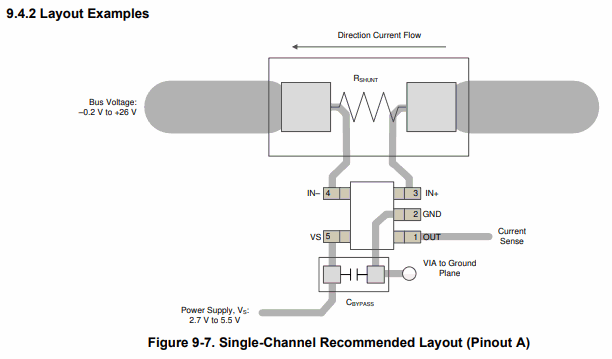
Pay attention to the application section of the datasheet: INAx180 (p.28)

enter image description here

A Kelvin connection is common practice for low-value shunt resistors, both to get a more accurate value of the resistor itself (four-terminal parts are also available for high accuracy purposes), and to avoid trace resistance effects as you have discovered.

Changing the layout as so is a straightforward fix:

enter image description here

You may want to adjust placement and pour geometry a bit to maintain ground fill around the components, and obviously the via under the INA180 has to move.

Note that your circuit may still be susceptible to EMC considerations, especially due to contact switching noise in the relays. A bypass capacitor on +12V and an RC snubber to GND on each output may be desirable for this reason.

Also, don't forget to stitch top and bottom ground fill with plenty of vias, particularly around trace crossings, inside corners, peninsulas, etc.

\$\endgroup\$

Your Answer

By clicking “Post Your Answer”, you agree to our terms of service and acknowledge you have read our privacy policy.

Not the answer you're looking for? Browse other questions tagged or ask your own question.