I am trying to design a high voltage (12V) buffer that will drive a sine wave with rail-to-rail peak-to-peak amplitude and a big capacitive load, maybe 3nF.
Browsing I came upon this Master's project: High Speed Digital CMOS Input Buffer Design by Krishna Duvvada
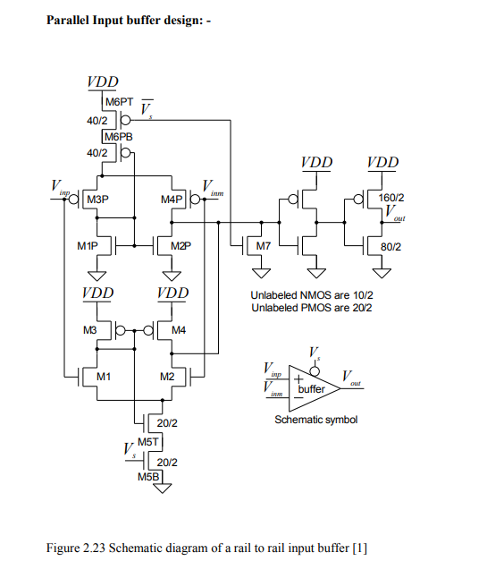
On page 14 (PDF page 30) there is a very basic rail-to-rail differential input, one with NMOS and other with PMOS for input pair, apparently self-biased, going over to two push-pull amplifiers buffering the output.
(This circuit is credited in the project paper footnote {1} to the book:
R. Jacob Baker, CMOS Circuit Design, Layout and Simulation, 2nd ed. Boise, ID:Wiley-IEEE, 2005.)
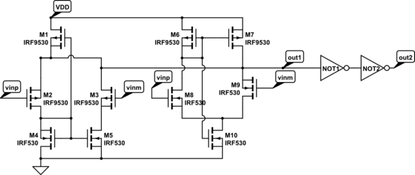
I tried setting this up in Cadence, with reference voltage connected to the inverting input, as described in the pdf.
The only thing I left out was the switch MOSFETs, the NMOS M7 after the first stage and the M6PT and M5B because I wanted to see the effect described and because for first time testing I didn't deem it necessary. Although, I have a question about those switches too.

simulate this circuit – Schematic created using CircuitLab
I just drew the schematic for easier referencing. I never used this tool though. I ended with two inverter symbols...
When I tested with reference voltage tied to inverting input, the results were ok.
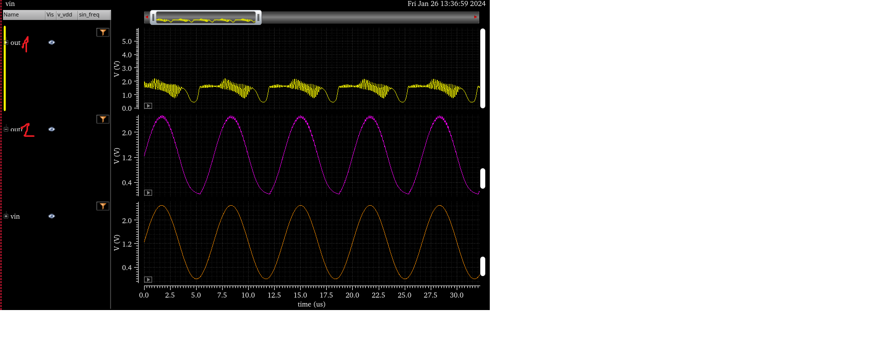
When I configured it as a buffer, with the inverting input connected to the output (out2 on my Circuit lab picture) I see a lot of ringing.
I seem to lack knowledge about this, so I would appreciate pointers too. Here are my questions:
- Why is there ringing? Where does it come from? You can see ringing at
out1which looks terrible and then there's little bit of ringing left on theout2(I didn't expect it to change so much atout2, I would appreciate a comment there too). - How can I get rid of it?
- The self-biased part of this circuit, I am not sure if this is a good way to do it. Doesn't it seem like, if done this way, the biasing transistors are always changing stable states? From what I see, they don't reach saturation, they stay in linear state. Judging by results, it seems kind of ok, the voltages seem high enough to have enough current, but I have a feeling there may be a better approach?
- It is supposed to be a buffer on a pad where size and consumption matter and with a big 3nF capacitive load, I would appreciate any ideas what to look into.


