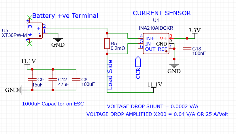
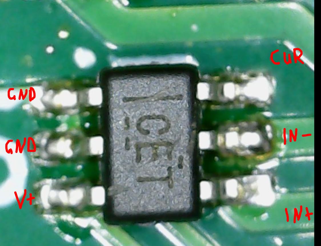
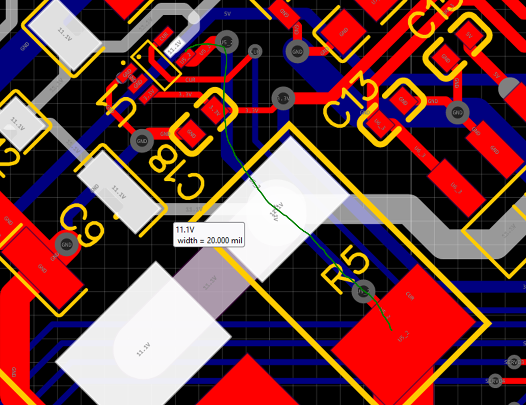
Now that you've included a picture of your layout it seems that the long trace going to U1 pin 5 may be a problem. (Barring any other potential problems already included in the comments.)
The trace connection going to the via under R5 already seems to be in the form of a Kelvin connection.
But before you actually redesign the whole PCB you could try to verify that the extra trace is the actual cause. To do this first cut the trace just after the pin edge of U1 pin 5, (without disturbing the traces beyond that).
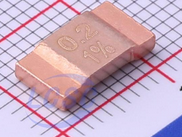
Tack solder a thin wire directly from U1 pin 5 to the pad of R5, (try connecting to the pad corner away from the other traces and use a very minimal amount of solder).
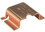
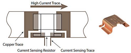
If you then test your PCB and find that you get results closer to what you expected you can be fairly sure that the extra trace length was causing the problem. You can then redesign the PCB to create a form of Kelvin connection to R5 similar to figure 3 in the Digikey link in the answer from Math Keeps Me Busy, (who should get the credit for explaining the concept). Alternately you might just order an actual shunt resistor that has the Kelvin format and use that instead.
Another issue that may effect the accuracy of using such a low value shunt resistor could be from running traces in different directions off the pads. Ideally you want all of the current that is to be sensed running directly and evenly across the resistor. If there are traces with currents going off at multiple angles from the pad (as you currently have), there could be small voltage drops across the pad itself. If you do redesign the PCB layout you may be able to reduce additional errors by using a single centered trace for the high current going to and from each pad of the shunt resistor, then create the traces to the sense chip as shown in the Digikey link.

