4
\$\begingroup\$

Are the dies made for a BGA package any different from the dies for a QFN or a DIP Package? Do BGA dies have connections on the lower side of the die? In the substrate?

How are terminals put in the package under the die?

I came across this picture. Are BGA packages actually PCBs? and are signals just taken off the die edge and routed to the bottom of the package? If so, how does this help in decreasing inductance at high frequencies?
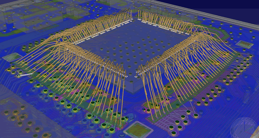
BGA image

I also came across the image below which makes it look like the BGA packages have connections from the bottom side - from the substrate.
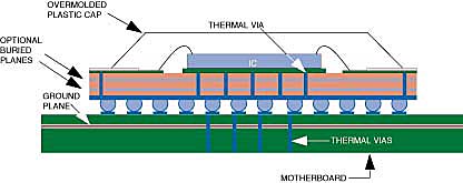
BGA Cross section

\$\endgroup\$
4
  • \$\begingroup\$ It helps that the die for a Cortex A9 is only 15% of the side length of the package it's in (less than half of what your picture shows). \$\endgroup\$
    – τεκ
    Commented May 23, 2013 at 20:34
  • 2
    \$\begingroup\$ Many BGA dies are also mounted flip-chip, with "C4" joints: en.wikipedia.org/wiki/Flip_chip \$\endgroup\$
    – Shamtam
    Commented May 23, 2013 at 23:29
  • \$\begingroup\$ @Shamtam - Okay! So that is what Flip Chip means? The Die is flipped to substrate top and etched layers at the bottom? I guess the package should not be different. Are they? BGA & FC-BGA? \$\endgroup\$
    – Lord Loh.
    Commented May 24, 2013 at 4:12
  • \$\begingroup\$ BGA refers to the entire package, the die on the BGA may be mounted with wire-bonding, or flip-chip, etc. After re-reading my last comment, i realize it was kind of unclear. \$\endgroup\$
    – Shamtam
    Commented May 24, 2013 at 12:53

2 Answers 2

5
\$\begingroup\$

Yes, BGA packages are like little circuit boards. On high pin count devices, in nearly all cases, the balls that lie directly under the die are mostly ground (and sometimes power) connections. The ground balls are fed directly through to the substrate of the die, while the power balls connect to internal power planes. Also, because of their direct metallic connection to the die, the ground balls help remove heat from the package.

All of the I/O is connected to balls near the periphery of the package, keeping their internal traces — as well as the PCB traces they connect to — shorter and inductances lower.

\$\endgroup\$
3
\$\begingroup\$

At the silicon level, you plan to have pins exposed to the outside. The die is pretty much always significantly smaller than the actual, package, so to connect to the pins, bond wires are used.

The layout is performed with an idea of where each bond wire is going to go, to give the shortest bond wire for minimal length. On a BGA package, there are no pins on the edge, so all the bond wires have to travel less distance, meaning less overall inductance. More critical pins will generally have the shortest bond wires (or even none at all), and those towards the outside of the package will be less critical as far as inductance is concerned.

Generally you'll see VCC and GND pins on the inside, as those want to get to the power planes of the PCB with minimal induction, and IO Pins more towards the outside to minimize trace length on the PCB which will contribute far in general than the induction of the bond wires.

BGAs are not necessarily going to have a PCB type layer on them, that is usually on very high pin count devices such as modern processors, which include their own on-board decoupling capacitors.

\$\endgroup\$

Your Answer

By clicking “Post Your Answer”, you agree to our terms of service and acknowledge you have read our privacy policy.

Not the answer you're looking for? Browse other questions tagged or ask your own question.