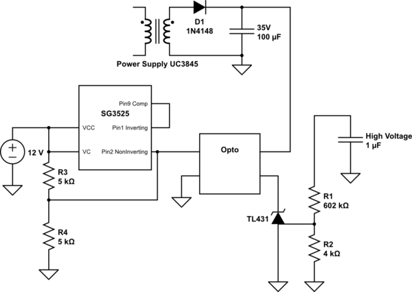
This is from a UPS which creates 350VDC from 12VDC, How does this arrangement work to control presumably the duty cycle of SG3525?
Compensation (pin 9) and inverting input (pin 1) are connected directly together, non-inverting input (pin 2) is connected to the optocoupler and has a 5k+5k voltage divider to VCC, which at 12 V from battery would create 6 V which should be under 5 V?
I tried looking for similar designs but failed to find one, if powered, circuit does create under 100 VDC on the output that slowly climb in 10 seconds or so.
I know there is a sawtooth oscillation that is compared with error amplifier, if Non Inverting input is pulled low duty cycle should decrease but I am already getting barely any output. Please help me understand this design.
Update: Managed to trace it using bright light under pcb and scratching traces at possible paths. Now schematic is more accurate.

simulate this circuit – Schematic created using CircuitLab
