0
\$\begingroup\$

To turn on the N-channel MOSFET on the high side, a higher voltage against source terminal must be applied to its gate terminal. Usually we use an extrenal driver or charge-pump.

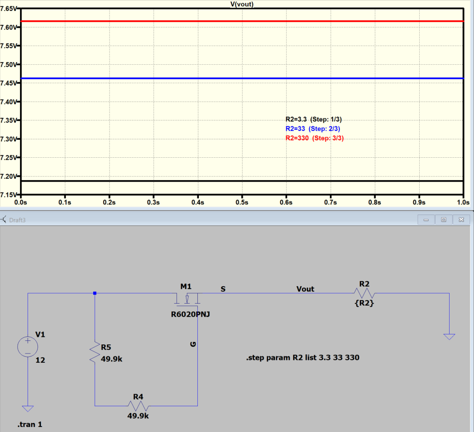
Is there any application for below circuit which has a high-side N-MOSFET without a driver or charge pump? I see relatively constant output volatge independent of load resistance.

Ofcourse if input voltage varies, nothing much we gain. The output also varies accordingly. Vout= Vin-~Vgs(th)

enter image description here

\$\endgroup\$
6
  • \$\begingroup\$ In what context, linear? Switching? What tradeoffs or penalties might this incur, when would it be a problem, and how worthwhile would it be to address it? \$\endgroup\$ Commented Apr 2 at 8:40
  • 1
    \$\begingroup\$ Do you notice the almost 5 V drop across your N-MOSFET? \$\endgroup\$
    – winny
    Commented Apr 2 at 8:52
  • \$\begingroup\$ @winny: Yes. If the current is low, it should be ok, right? Just like a variable power resistor or LDO. \$\endgroup\$ Commented Apr 2 at 8:57
  • \$\begingroup\$ @TimWilliams: Linear ofcourse, else it would never be able to turn ON. \$\endgroup\$ Commented Apr 2 at 8:59
  • \$\begingroup\$ But you say in the title "still turns ON" -- which one is it? The deeper realization seems to be, "on" is a matter of degree. Perhaps you could rephrase your question under this perspective? \$\endgroup\$ Commented Apr 2 at 9:05

3 Answers 3

1
\$\begingroup\$

In a synchronous boost converter when vin ~ vout, there may be insufficient time to ramp inductor current down without impacting switching frequency. If that is not desired, ‘diode’ connecting the synchronous MOSFET will increase the voltage across the inductor, resulting in a quicker discharge.

\$\endgroup\$
0
\$\begingroup\$

Is there any application for below circuit which has a high-side N-MOSFET without a driver or charge pump?

I use a similar circuit (yes, not exactly the same circuit) as some sort of "clamper" in one of my designs: I keep the gate voltage constant and I make use of the body diode to decide when to switch on or off the MOSFET.

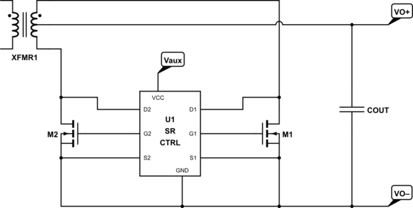
Below is a simplified schematic of the secondary-side sync-rectifier (SR) of the converter (a resonant converter, by the way):
schematic

simulate this circuit – Schematic created using CircuitLab

The U1, SR controller, takes D (drain) and S (source) connections of the SR MOSFETs as inputs, and outputs G (gate) voltages to drive the MOSFETs. And this particular IC uses a sophisticated method to drive the MOSFETs so it needs to measure the drain voltage when the respective MOSFET is on.

The voltages at the opposite ends of the secondary winding are out of phase and have opposite signs w.r.t. the centre-tap. So, when one winding has negative voltage the respective SR MOSFET's body diode will be in conduction, and the controller IC will catch this and turn the MOSFET on. And whilst the MOSFET is on the drain voltage will be negative. And when the winding voltage increases (rising edge) the IC will catch this as well and turn the MOSFET off.

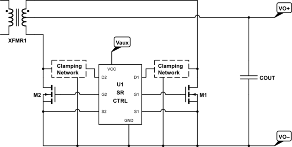
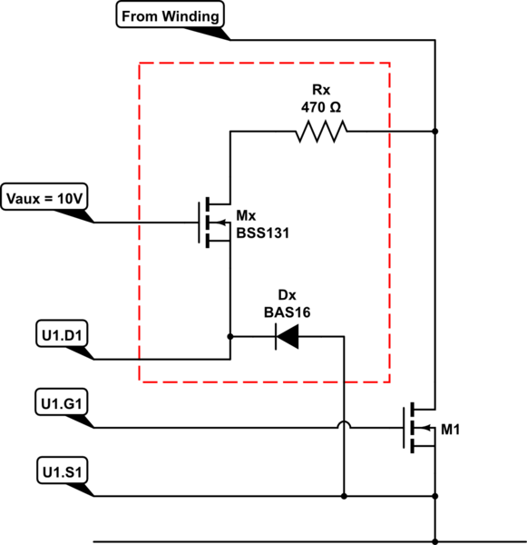
The MOSFET with positive winding voltage should stay off but its drain stress will be more than twice the output voltage. So, for a converter with 56V output, the IC's D pins will see ~120V. But the IC allows a maximum of 100V. We can't use a simple dropper (series Zener or voltage divider) because, even though the positive voltage level is not relevant for the IC, it requires the exact negative voltage when the MOSFET is on. So I put a circuit which I'd like to name as "positive-clamper-negative-passthrough" to protect the IC:
schematic

simulate this circuit

And here's the clamper section (shown one side only, the other side has the exact same circuit):
schematic

simulate this circuit

The circuit above basically clamps the voltage seen by the IC at its D pin at around Vaux as the circuit operates as a source follower (a.k.a. common drain).


Can still be considered as a high-side MOSFET, and is not driven with bootstrapping.

\$\endgroup\$
0
\$\begingroup\$

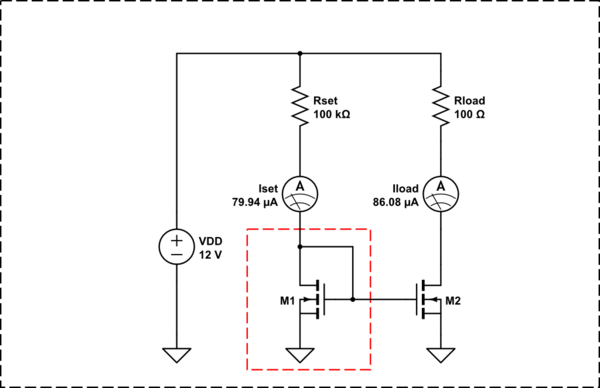
I see relatively constant output voltage independent of load resistance.

Indeed this circuit (red box below) is extensively used as a "diode-connected MOSFET" in analog ICs. Typically there are no resistors between gate and drain though, merely a direct connection. The usefulness comes from creating a voltage drop equivalent to what will allow a similar MOSFET to conduct a similar current even when the load resistance is different by orders of magnitude, i.e. a "current mirror":

schematic

simulate this circuit – Schematic created using CircuitLab

\$\endgroup\$
1
  • \$\begingroup\$ Altough keep in mind that, just as with the bipolar equivalent, proper operation requires a very high degree of device matching. Generally speaking, this sort of geometry is only useful with FETs which are at least part of the same die, and for high-precision use the two have to be carefully designed so as to give the same effective temperature across both devices. \$\endgroup\$ Commented Apr 3 at 14:09

Your Answer

By clicking “Post Your Answer”, you agree to our terms of service and acknowledge you have read our privacy policy.

Not the answer you're looking for? Browse other questions tagged or ask your own question.