3
\$\begingroup\$

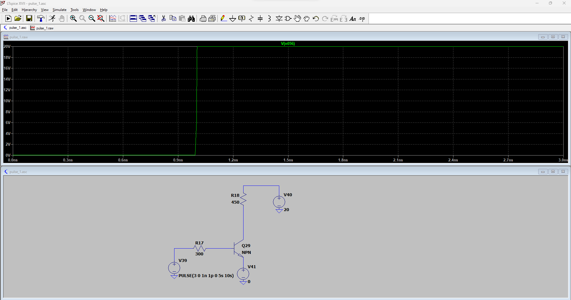
I need a fast +,-10 V pulse. I thought I could trigger the base of a switching transistor with my fast rise time digital I/O and get a 0-20 V at the collector and then shift the DC to 0 volt and have a symmetrical +,-10 V pulse. The first part of creating the 20 V pulse is easy. But is there an easy way to shift its DC to 0 volt?

I can't use op-amps, because they would deteriorate the rise time of the pulse. I want the rise time to be kept below 10 ns. Comparators with such fast rise time and high supplies are I guess not available as an IC. So probably I need a discrete solution.

Simulated step response of an NPN BJT-based common-emitter amplifier, exhibiting the risetime

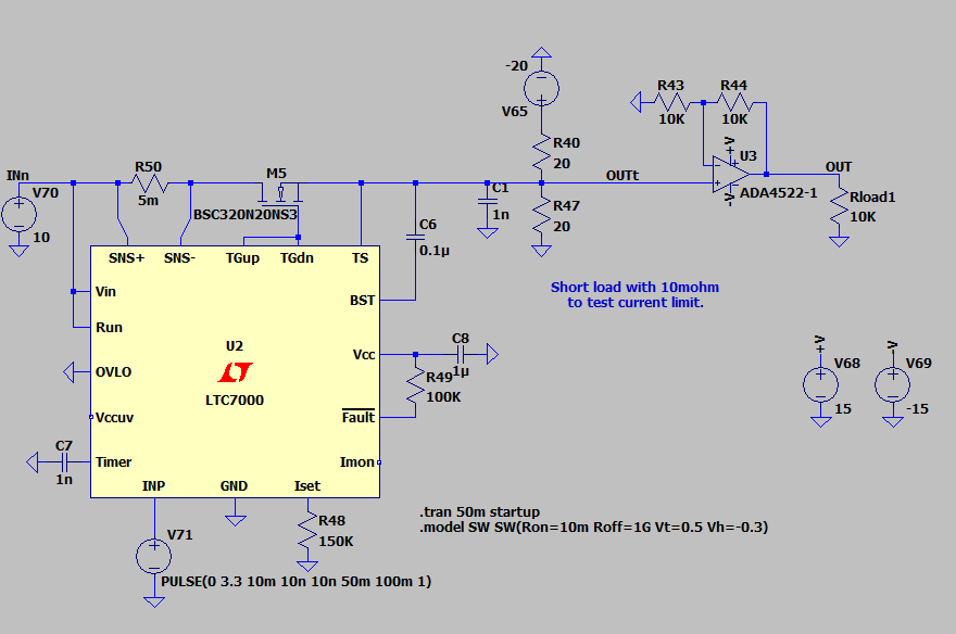
I want to use the generated pulse for measuring slew rate of an op-amp. Based on a suggestion in a comment, I used a gate driver:

A schematic diagram with an LTC7000

\$\endgroup\$
8
  • \$\begingroup\$ What supply voltage(s) do you have? 20V only? \$\endgroup\$ Commented Apr 20 at 6:13
  • \$\begingroup\$ @RohatKılıç, I have +, - 10V also. \$\endgroup\$
    – Fateme
    Commented Apr 20 at 6:16
  • 1
    \$\begingroup\$ Does the ±10V output have to be ground-referenced? Are you okay with having that swing across a non-ground-connected load? \$\endgroup\$ Commented Apr 20 at 6:24
  • \$\begingroup\$ @RohatKılıç yes, the swing needs to be ground referenced. \$\endgroup\$
    – Fateme
    Commented Apr 20 at 6:32
  • 1
    \$\begingroup\$ My first thought would be an AC coupling capacitor. Very widely used on GHz clocks. \$\endgroup\$ Commented Apr 20 at 15:29

5 Answers 5

7
\$\begingroup\$

Seems a MOSFET gate-driver will meet your requirements. There are many examples of complete one-chip solutions that accept a logic-level input, and convert this to a level-shifted version with a slight time delay (<100ns) , with very fast rise/fall times (less than 20ns in many cases) and capable of delivering several amps of current into a capacitive load.

Many suitable examples will be found when you search the various electronics suppliers using search phrases such as "MOSFET Gate driver", & "logic clock driver".

However, many of the more commonly available options have a maximum output voltage limit of +15V; to deliver +/-10V (20V) reliably with some margin I would choose a unit with max Vcc > 23V; the available options meeting this rating are less common. The newer chips designed to drive SiC MOSFETs tend to have output drive capability up to +30V, however, these are more expensive than the older, lower voltage devices.

Here are some examples to consider, sorted by max output V (ascending), note that "C-load" is the load capacitance connected to test the rise/fall times (as mentioned in the datasheet); I suspect the rise/fall times you will see will be shorter (faster) since your application does not have a large capacitive load.

# OEM Part no max output V delay time rise/fall time C-load
1 TI UCC2732x 16V 25ns 20ns 1.8nF
2 ON-semi NCP51530 20V 60ns 8ns 1nF
3 ON-semi MC34151 20V 35ns 15ns 1nF
4 Diodes Inc DGD0215/0216 22V 35ns 15ns 1nF
5 ON-semi NCP51705 28V 25ns 8ns 1nF

Above: Table 1

The previous table shows non-isolated chips where the input and output share a common 0V connection; to get +/-10V output using these chips requires AC coupling the output (or input) and perhaps some DC restoration. Alternatively, there are gate driver chips that include an isolation barrier between the input and output; this will allow the input pulse to be ground referenced, while the output is referenced to a negative supply (ie: the output switches between -10V & +10V). Here are some examples to consider:

# OEM Part no max output V delay time rise/fall time C-load
1 Skyworks Si8285 30V 40ns 5.5ns 200pF
2 Analog Devices ADuM4146 30V 75ns 15ns 2000pF
3 Infineon 1EDI20N12AF 40V 120ns 10ns 1000pF

Above: Table 2

The figure below is from the datasheet for Infineon 1EDI20N12AF, showing how to connect the positive & negative supplies to the output section via pins VCC2 & GND2. The input section is fed from a separate logic-level supply via pins VCC1 & GND1.
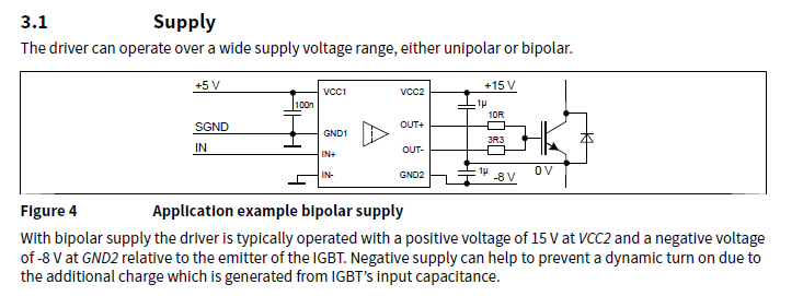
enter image description here

If you select the Infineon device, to adapt it for your application I suggest doing the following:

  1. The diagram shows an IGBT connected to the output; remove this and replace it with your circuit under test.
  2. Connect the node marked "0V" to node "SGND".
  3. Connect VCC2 to +10V, and GND2 to -10V.
  4. Use good capacitors to filter the power supply, and locate these very close to the chip; minimise the current path loop area formed by the bypass capacitors and the chip.
\$\endgroup\$
7
  • 1
    \$\begingroup\$ Most drivers will deliver a plenty sharp output, if lightly loaded, or resistive; notice the rise/fall is usually specified into a nominal load e.g. 2nF or whatever, and driving such a load to under 20ns is quite some (peak) effort, but when lightly loaded, the risetime is limited more by the chip's internal driving transistors, which can be quite fast. IXYS's higher voltage drivers (IXDD609CI, etc.) for example, may therefore be contenders. \$\endgroup\$ Commented Apr 20 at 11:33
  • 1
    \$\begingroup\$ @TimWilliams actually I want to use this pulse as an input pulse for measuring slew rate of an op-amp. since the output of a gate driver like LTC7000 is not ground referenced, can I add a resistor divider(with small resistors) at the output of the gate driver connected to a negative voltage? and then connect it to the input of the op-amp? I edited the question with a picture of what I mean \$\endgroup\$
    – Fateme
    Commented Apr 20 at 12:16
  • 1
    \$\begingroup\$ @Fateme Many gate driver chips include an isolation barrier between the input and output; this will allow your input pulse to be ground referenced, while the output is referenced to negative the supply (-10V). For example, Skyworks produces a range of products with an isolation barrier capable of blocking several hundred volts. They have an extensive range, one example that may be suitable is the Si8285. I will add this to my answer. \$\endgroup\$ Commented Apr 20 at 19:50
  • \$\begingroup\$ @Fateme This would've been important context to include in the original post, as the DUT can be wired common-ground and operated from a e.g. 20-30V supply. It can also trivially be AC-coupled and run from any supply. \$\endgroup\$ Commented Apr 20 at 21:41
  • \$\begingroup\$ @FabioBarone A: Should I use isolated DC-DC converters for the gate driver for the high-voltage part? like I mean a +/-supply or separate ground referenced +Vs and -Vs supplies? B: if I connect 0V to SGND, it is no more an ISOLATED gate driver, is it? \$\endgroup\$
    – Fateme
    Commented Aug 10 at 8:02
2
\$\begingroup\$

So the rise time is your only concern and neither the delay nor the pulse stretching is your problem.

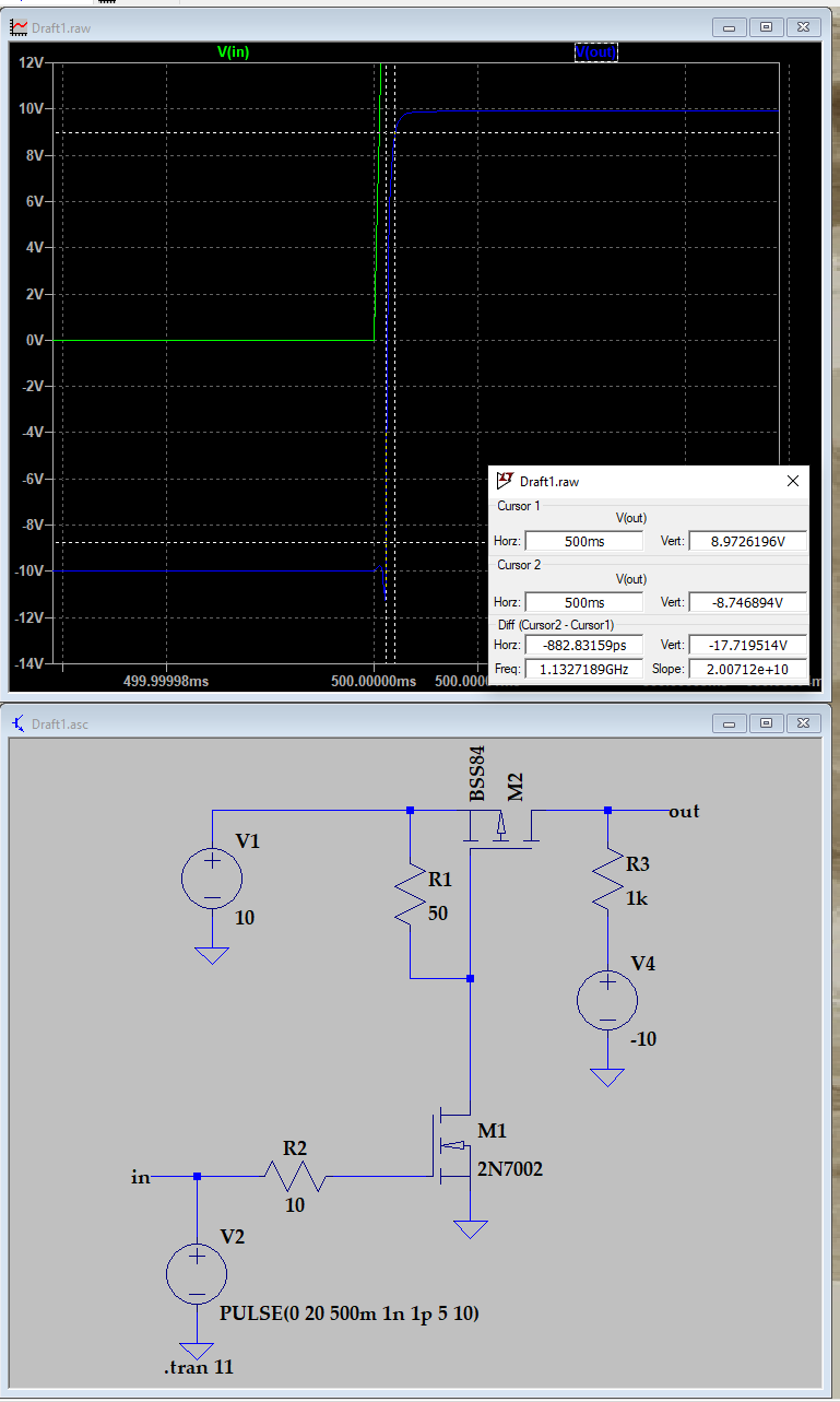
To give a rough idea, I'm leaving a very simple circuit below consisting of MOSFETs with very low Ciss or QG such as 2N7002 and BSS84:

enter image description here

As you can see, the rise time is almost unchanged. 2N7002 can withstand continuous gate-source voltage of 20V and pulsed gate-source voltage of 40V, so it's safe to drive with 20V directly. The problem with this circuit is, obviously, that it's lossy:

  • Because R1 interacts with M1, it has to be kept low (Increasing it changes the output rise time). Average dissipation, according to LTspice, goes slightly above 1 W.
  • The peak gate currents for 7002 can reach 1 Amps (I put 10 Ohms of gate resistance randomly but you can increase until the rise time goes beyond your requirements). Considering the 120-Ohm internal gate resistance of 7002, the peak losses will be high. LTspice gave a total avg loss of less than 50 mW for that part, though.
\$\endgroup\$
7
  • \$\begingroup\$ Thank you, R3 should be a 20W resistor. seems impossible on a PCB? \$\endgroup\$
    – Fateme
    Commented Apr 20 at 11:21
  • \$\begingroup\$ @Fateme load resistor doesn't matter. I just put a random load resistor. Can be even 100k. \$\endgroup\$ Commented Apr 20 at 11:45
  • \$\begingroup\$ @Fateme if you think about making this circuit on a PCB, consider trace inductance and trace capacitance (i.e. trace-to-trace or trace-to-plane capacitance for multi-layer PCB). \$\endgroup\$ Commented Apr 20 at 11:50
  • 1
    \$\begingroup\$ @Fateme ±10V doesn't dissipate 20W across a 100k resistor. \$\endgroup\$ Commented Apr 20 at 12:13
  • 2
    \$\begingroup\$ @Fateme and this verifies that a 100k resistor doesn't dissipate 20W. I initially put 1k as a load, just a random value, and yes it dissipates 20W but it doesn't have to be 1k. With 100k load you'll still get your fast rise time and the dissipation across it will be much lower. \$\endgroup\$ Commented Apr 20 at 12:31
2
\$\begingroup\$

It looks like job for "gate driver". What about to take some 20V+ gate driver like Si8261 (or many others) ? Its rise/fall time is under 10ns, amplitude can be set by supply voltage. Thanks to galvanicaly isolated input you can tie its VDD to +10V and GND to -10V and your input signal still can be refered to your GND (0V).

\$\endgroup\$
2
\$\begingroup\$

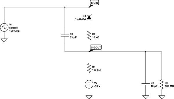
We had a project where we needed to replace a rather power hungry dedicated levelshifter with an alternative. In the end we came up with the following idea:

schematic

simulate this circuit – Schematic created using CircuitLab

It is an extention to the common zener diode levelshifter approach. The additional cap ensures that the AC part of the signal is transferred fast enough and not low-pass filtered by the parasitic RC-filter. It can be seen as an AC voltage dividers formed by the caps and a DC voltage divider formed by the resistors. The exact values are strongly dependent on the parasitics and input impedance and power budget. This circuit "abuses" the fact that the inputs have clamping/ESD diodes in place. R2 effectively limits the current during the "high" state but at the expense of a reduced signal amplitude because of the voltage divider. We use a SN74 based buffer to sanatize the signals afterwards and keep the trace parasitics in check, but this would be too slow in your case.

\$\endgroup\$
2
  • 1
    \$\begingroup\$ The 100 GHz needs an explanation. For instance, supposedly, all physical dimensions become important. The wavelength (in vacuum) is 3 mm at 100 GHz. \$\endgroup\$ Commented Apr 20 at 23:31
  • \$\begingroup\$ Good point. I just put a random high frequency. Had 1 GHz first because if the signal flank is 10 ns a 10x wider BW seemed reasonable. But it was late and somehow I mixed up orders of magnitude during reviewing the post and changed it. As mentioned: exact values depends on the parastics/layout. \$\endgroup\$ Commented Apr 21 at 9:43
1
\$\begingroup\$

You could use a capacitor with clamping diodes at the output side to maintain the correct DC levels, but that only works if you have repeating pulses with sufficiently high frequency, not of there are long periods without activity. So it depends on your pulsed signal whether this is possible, but it's the simplest solution.

Or you could just use an opamp with +10V and -10V supply rails. That would work for any sequence of pulses.

As an alternative you can build your own opamp, with probably at least 3 or 4 transistors, but that's already a big project where many things can go wrong.

\$\endgroup\$

Your Answer

By clicking “Post Your Answer”, you agree to our terms of service and acknowledge you have read our privacy policy.

Not the answer you're looking for? Browse other questions tagged or ask your own question.