2
\$\begingroup\$

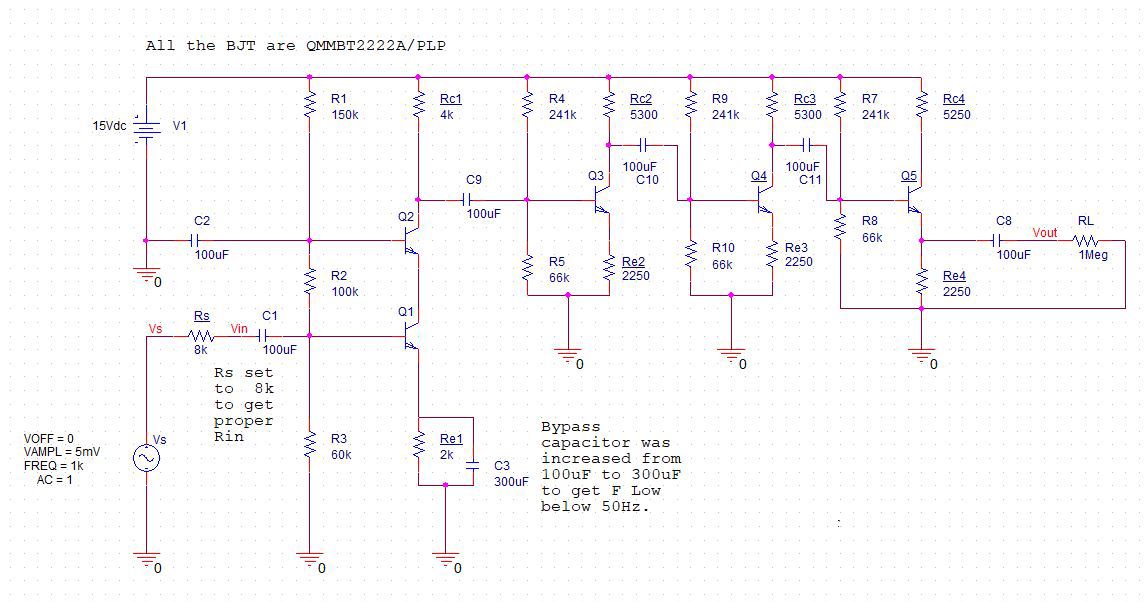
I designed a multi-stage amplifier (I know, so original) for my circuits class. It follows all the parameters that are needed:

  • Vs (sine wave) of 10 mV pk-pk
  • Vdc of 15 V
  • Gain of -250 without load (2.5 V pk-pk) / inverted
  • Rin > 10 kΩ
  • Ro < 50 Ω
  • Lower cut-off < 50 Hz
  • Upper cut-off > 150 kHz.

The last part of this lab is the issue. When I add a 100 Ω resistor at Vout, I need a gain of around -200 (2 V pk-pk) and Vs can be adjusted a little bit to get that value.

BUT, my circuit is clipping during the negative portions of the signal. Why?

All transistors being used are 2N2222 BJTs. Stage 1 is a cascode amp to reduce the Miller effect, stage 2 and 3 are CE for more gain, and stage 4 is for a low output impedance.

enter image description here

\$\endgroup\$
10
  • \$\begingroup\$ Please share the complete set of requirements for the amplifier, as well as the constraints. Why did you change load to 100ohm from 1 meg ohm? \$\endgroup\$ Commented Apr 21 at 5:15
  • \$\begingroup\$ This was the complete set of requirements. This was all that was instructed. And I changed the load from 1 Meg (No Load in Spice) to 100 Ohms because that's what was instructed of me to do. \$\endgroup\$
    – Boost
    Commented Apr 21 at 5:18
  • \$\begingroup\$ So, to be totally clear: You have mentioned two requirements; "Gain of -250 without load (2.5V Pk to Pk) / Inverted" AND "Gain of -200 with load = 100 ohm. Are both of these requirements to be met simultaneously? \$\endgroup\$ Commented Apr 21 at 5:39
  • \$\begingroup\$ Q2: were you constrained to using a multi-stage set of C-E amplifiers, or were you given freedom to pursue any amplifier architecture you wanted? Q3: Is there an upper limit on the number of components (eg: Rs, Cs, and transistors)? Q4: Can you use dual pos and neg power supplies, or are you constrained to having just one? \$\endgroup\$ Commented Apr 21 at 5:44
  • 2
    \$\begingroup\$ First, remove Rc4 (replace it with a short circuit.) and change R7 value to 56k. \$\endgroup\$
    – G36
    Commented Apr 21 at 6:28

3 Answers 3

3
\$\begingroup\$

goals

The specifications of \$A_v=200\$ (\$\approx 46 \:\text{dB}\$) into \$R_{_\text{L}}=100\:\Omega\$ with \$v_{_{\text{IN}_{PP}}}=10\:\text{mV}\$.

Calculates out to \$v_{_{\text{OUT}_{PP}}}=2\:\text{V}\$. So \$v_{_{\text{OUT}_{PK}}}=1\:\text{V}\$ and \$i_{_{\text{OUT}_{PK}}}=10\:\text{mA}\$.

This also means delivering only \$5\:\text{mW}\$. I'll avoid class-AB. Too much to discuss. And stick with class-A. Fewer quantitative details to worry over.

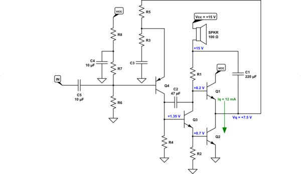
class-A template starting point

Here's the starting template:
schematic

simulate this circuit – Schematic created using CircuitLab

(I'll be using E24 resistor values [5% tolerance]: 1.0, 1.1, 1.2, 1.3, 1.5, 1.6, 1.8, 2.0, 2.2, 2.4, 2.7, 3.0, 3.3, 3.6, 3.9, 4.3, 4.7, 5.1, 5.6, 6.2, 6.8, 7.5, 8.2, 9.1.)

The speaker is bootstrapped by \$C_1\$. This has the advantage of arranging things so that \$R_1\$ can act as a current source. (If you follow the voltages around the loop there, you will see why.)

\$R_5\$ provides global NFB, in conjunction with \$R_3\$. (\$C_3\$ needs to be an effective short at some desired high-enough frequency.) This is how we will set the closed loop voltage gain, \$A_v\$.

\$Q_1\$ and \$Q_2\$ are the 2-quadrant class-A output driver pair and I've centered the midpoint of their output to halfway between the rails. I chose \$I_{_\text{Q}}=12\:\text{mA}\$ and they will each dissipate an average of \$90\:\text{mW}\$. Even without plated through-holes to help, temperature rise should be under \$20^\circ\$C over ambient for small-signal TO-92 packaging. So these are any of 2N2222A, PN2222A, P2N2222A, or 2N3904 (or many others of similar availability for small signal use.)

note on \$V_{_\text{BE}}\$ values

The increase in \$V_{_\text{BE}}\$ due to \$I_{_\text{Q}}=12\:\text{mA}\$ will be compensated by the \$20^\circ\$C rise over ambient so I'm going to just call it as \$V_{_\text{BE}}=700\:\text{mV}\$ for \$Q_1\$ and \$Q_2\$ and set the base voltages as shown above. \$Q_3\$ will probably be closer to \$V_{_\text{BE}}=650\:\text{mV}\$, so I plugged that base voltage into the schematic above, as well.

cross-over at \$150\:\text{kHz}\$

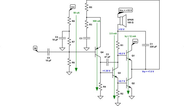
The part of the design that is going to drive me away from the rule-of-10's in biasing the BJTs is the elephant in the room: the cross-over at \$150\:\text{kHz}\$. I want to use a \$47\:\text{pF}\$ Miller cap for the \$Q_3\$ VAS, to manage its parasitic capacitance. But this also means I need to run things hot so that \$R_4\$ can be made small enough.

Given this is already a highly inefficient class-A, running it hot it won't even be noticed. So here's the updated version:
schematic

simulate this circuit

That is, without a doubt, insanely hot. But it is the \$500\:\mu\text{A}\$ current that I'm targeting because of \$C_2\$ and because of the \$150\:\text{kHz}\$ cross-over. Better safe than sorry. And with the class-A, it's not going to be noticed that I'm over-doing this to get the needed bandwidth.

some added details

\$26\:\text{mV}\$ at the \$Q_3\$'s base gives me a 10-fold collector current change. I don't think I'll need more. So I might consider \$Q_4\$'s emitter at \$2.5\:\text{V}\$, tentatively, and its base at \$1.8\:\text{V}\$. So it's time to go work out \$Q_4\$'s biasing.

Looks like I can use \$R_6=R_7=36\:\text{k}\Omega\$. \$R_8\$ doesn't work out quite so well, but I'll select \$R_8=240\:\text{k}\Omega\$. That sets \$Q_4\$'s base to \$1.73\:\text{V}\$. Let's update the schematic:
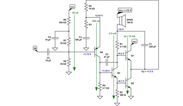
schematic

simulate this circuit

I've filled in a bunch more values. I won't explain all of them, as they fall out from the information already determined for the schematic. All I was doing is doing a short calc, selecting a nearby E24 value, and stuffing them in. I did update \$C_3\$. It will need to be hefty.

\$Q_4\$'s \$r_e^{\:'}\approx 50\:\Omega\$, so I know \$R_3\lt 50\:\Omega\$ (\$R_5\$ divided by the gain of 200) may need to be just a little lower. But not much. In any case, that's part of the process once this is built to achieve the designed voltage gain.

validation through simulation

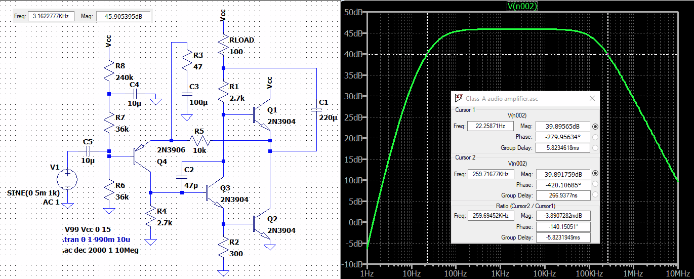
I'm going to plug this into LTspice and tweak \$R_3\$, once there, to get the voltage gain about right. My first guess will be \$R_3=47\:\Omega\$. At this point, I'm scared I missed some important detail. But hopefully, I will get lucky and have covered the important details without error! We shall see:
enter image description here

As you can see in the upper-left corner, it's getting about \$45.9\:\text{dB}\$ into a \$100\:\Omega\$ load. That's \$A_v\gt 197\$. I call that good. I could adjust \$R_3=43\:\Omega\$ to push \$A_v\$ well over the top. But I won't bother. Looks like I saved myself from a redo!

Also, note that the \$-6\:\text{dB}\$ corners are better than spec'd. This means I would either boost \$C_2\$, but may need to find an odd value as I think going to \$100\:\text{pF}\$ might be over-kill. Or else cool it down a bit so that \$R_4=4.7\:\text{k}\Omega\$, \$R_5=18\:\text{k}\Omega\$, and \$R_3=82\:\Omega\$. And that gets the high end. \$C_5\$ could be cut down to about \$150\:\text{nF}\$ to roll off on the low-end at about \$50\:\text{Hz}\$.

These last details are all tweaks I'd do, once the circuit was built, and before presenting it to a teacher for evaluation. They may be impressed with the accuracy and attention to specification details.

schematics note

A schematic sheet should be viewed as a curtain of currents flowing from top to bottom, with signals using that flow to allow themselves to travel across the curtain from left to right. If the above schematic process doesn't manage to clarify that basic idea, nothing else will.

\$\endgroup\$
1
\$\begingroup\$

I would start with designing the output stage; this would be a voltage follower unity-gain stage (an emitter follower, or common-collector). I would prefer to use split power supplies because that eliminates the output DC-blocking capacitor. Focus on getting the biasing of this stage correct when there is no signal (ie: signal is 0V). This stage is intended to provide all the load current, without loading down the previous stage.

Here is one idea you can use for this output stage:
https://electronics.stackexchange.com/a/689296/341959

I would then design a simple multi-transistor "op-amp" and apply negative feedback to get the necessary voltage gain of 250 (not 200) with a load of 100r. This could be as simple as a diff pair, followed by a C-E voltage amplifier stage (VAS). Various improvement to the VAS can be made, such as boot-strapping the collector resistor, or using a constant current load.

If the output stage is a good design, then the overall gain at no-load and at full load (100r) will be the same: 250. Using garden-variety small-signal BJTs such as BC549/BC559 would get you a decent "op-amp"; the question will be whether the upper cut-off frequency (150kHz) will be met. You can then use the rather relaxed mid-band gain requirements (250 at no-load, 200 with load) to basically "relax" the bandwidth requirements of your amplifier.

If you find upper bandwidth requirement is still not met, you may find that one stage will dominate the bandwidth: it will be either the differential input stage, or the VAS. In this case, simply apply a cascode (common-base) to that stage.

Here is a link to this exercise:
https://electronics.stackexchange.com/a/688822/341959

\$\endgroup\$
6
  • \$\begingroup\$ It's like 8 mW into 100 Ohm! Simple 4 BJT class-A with global NFB to set the gain (among other benefits.) That's all, I think. \$\endgroup\$ Commented Apr 21 at 18:11
  • \$\begingroup\$ @periblepsis Well, 1V peak into 100ohms is 10mA, so the class A output stage idle current would need to be set at least 11mA, which means a constant power draw of 165mW from the 15V supply. A class AB output stage with a Vbe multiplier for biasing adds only 2 more transistors compared with a class A with a resistor bias; only 1 more with an active bias. I'd prefer a much lower drain on the battery than saving a couple of small-signal BJTs. As for the voltage amplifier, sure, a 2 transistor shunt-series feedback pair should work just fine, however I wanted to avoid coupling caps, & \$\endgroup\$ Commented Apr 21 at 21:48
  • \$\begingroup\$ ...I didn't have a SE reference handy to link to. Cheers. \$\endgroup\$ Commented Apr 21 at 21:52
  • \$\begingroup\$ I just look at that mess and recognize that the OP needs understandability. And the class-A is just easier to explain and get right without having to dial in crossover, for example. I hate the high dissipation, too. But in this case? High is still low enough to not worry about burning the house down. ;) \$\endgroup\$ Commented Apr 21 at 23:26
  • 1
    \$\begingroup\$ Even bootstrapped to increase input impedance! Cool. But... it is only one active quadrant and that 4.7k looks a little weak to me. :) I was thinking two active quadrants for the class-A. Something more like this. That thing goes back at least to the mid 1960's. \$\endgroup\$ Commented Apr 21 at 23:49
1
\$\begingroup\$

You've chosen to have a mostly fixed-gain architecture with no global feedback - I'll stick to that design then.

Input Stage

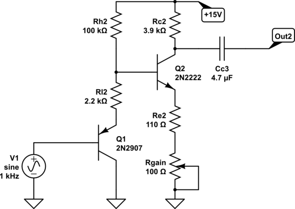
The cascoded input stage is a fair idea, but we can save a few components by using an emitter follower on the input and driving the first gain stage harder so that the Miller capacitance won't have much effect anymore.

This lets us DC-couple the input, and save some capacitors:

schematic

simulate this circuit – Schematic created using CircuitLab

The gain is 19x, constant from 0Hz to beyond 100kHz.

Output Stage

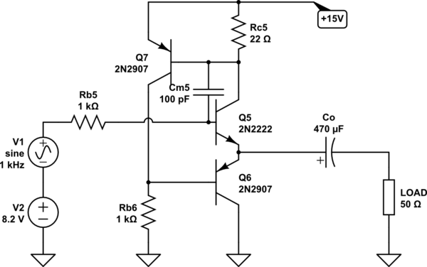
The output stage won't work as you've shown. You can have a low AC impedance (<<50Ω) output stage by establishing a fixed collector current on the output emitter follower Q5. There is a DC offset due to V(be), but that's constant, so only affects DC.

schematic

simulate this circuit

Even with a 50Ω load, the gain is very close to 1. That's because Q5's collector current is a constant 30mA, and thus the B-E voltage drop is just about constant as well. The output impedance is <1Ω as long as the instantaneous load current doesn't exceed 30mA. That's the case as long as the output voltage swing doesn't exceed 2.5Vpp with a 50Ω load. For lower load resistances, the idle current through Q5 would need to be higher, and you'd run out of the heat dissipation ability of a 2N2222.

Rc5 is a current sense resistor for Q5's collector. Q7 and Rb6 control the emitter load current generated by Q6. The control loop has negative feedback and establishes about 30mA bias current through Q5. To change Q5's operating point (bias current), adjust Rc5. The lower the Rc5, the higher Q5's idle current. Cm5 stabilizes the output stage and limits the bandwidth.

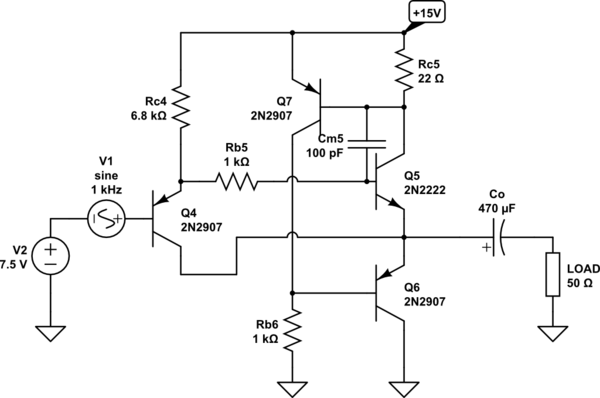
Since Q5's base drive needs source impedance on the order of 1kΩ, we have to add a follower buffer stage Q4:

schematic

simulate this circuit

The follower is bootstrapped to the output voltage. Rc4 sets 1mA bias for Q4. The bias likely can be lower than that.

Second Stage

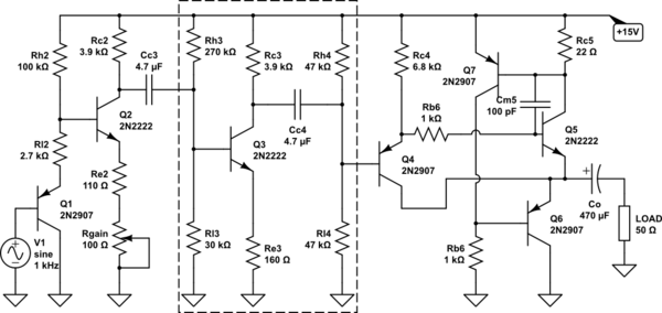
Next we can add another voltage gain stage, similar to how you've done it:

schematic

simulate this circuit

The coupling capacitors can be quite a bit smaller than the 100μF you've used. Foil or C0G/NP0 4.7μF will work well as shown.

Adjust Rgain for total gain of 250x at 10kHz.

Due to fairly low output impedance, the gain won't change much as the load impedance is changed. I.e. if you want to have 200x gain with load attached, just set the overall gain for 200x, not 250x.

\$\endgroup\$
3
  • \$\begingroup\$ I like that output stage, Vout is the same as Vin due to the opposite Vbe's of Q4 & Q5. And yes, the Vbe of Q5 is kept constant by the constant collector current of Q5, (the variation due to load current is pushed to Q6), which is nice. The complementary pair class-A output stage is interesting - I guess the advantage of it is it can be converted to a class AB output stage rather conveniently. Cheers. \$\endgroup\$ Commented Apr 21 at 23:50
  • 1
    \$\begingroup\$ @FabioBarone Making a class-AB stage that performs as well as a class-A stage is much harder, and would require many more components. Actively-loaded class-A is my go-to solution for high-performance low-power follower applications. It's of course best to have global negative feedback in an amplifier like this, but I wanted to at least get the original multi-stage, fixed-gain idea a chance :) \$\endgroup\$ Commented Apr 22 at 2:40
  • 1
    \$\begingroup\$ Agreed. We're not going for THD measured in parts per million here. Cheers. \$\endgroup\$ Commented Apr 22 at 2:54

Your Answer

By clicking “Post Your Answer”, you agree to our terms of service and acknowledge you have read our privacy policy.

Not the answer you're looking for? Browse other questions tagged or ask your own question.