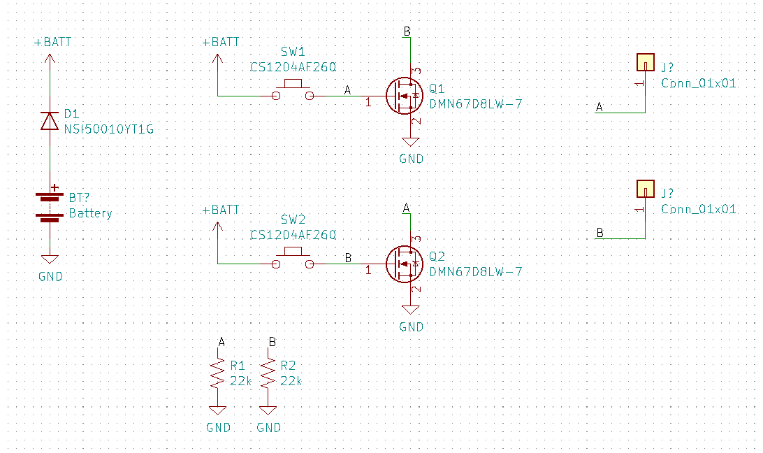
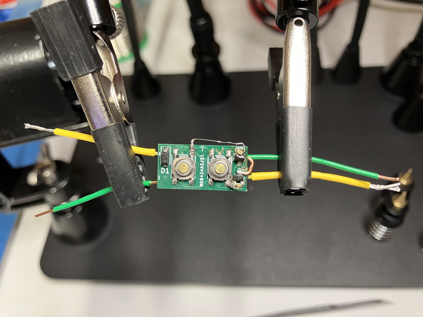
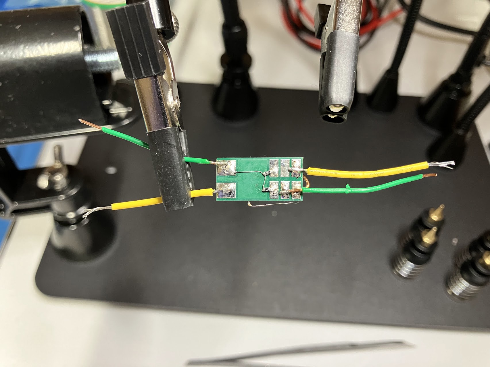
I have a three-state circuit which flips the polarity of a small resistive load using two push buttons.
The input is some battery voltage, between 10V and 25V DC. The output is two pins: A and B. The current limiter is about 10mA.
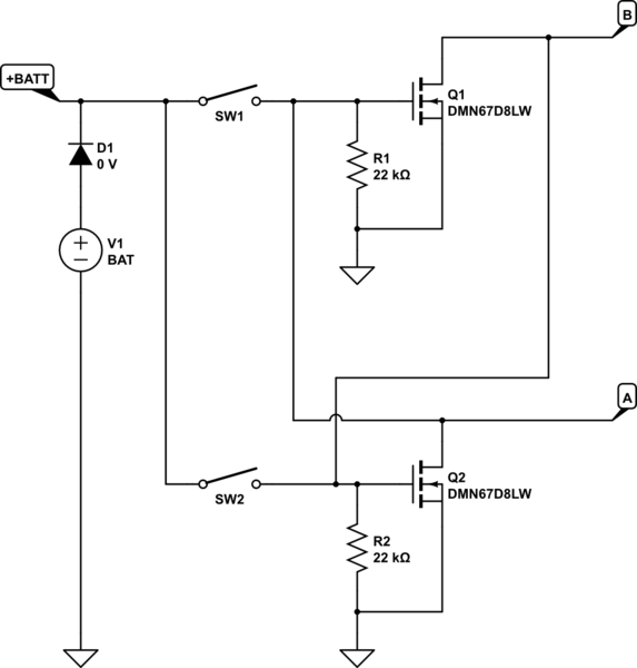
simulate this circuit – Schematic created using CircuitLab
Default state is VAB = 0V. When SW1 is closed, VAB = VBAT. When SW2 is closed, VAB = -VBAT. When both SW1 and SW2 are closed, the output is current-limited to 7 mA and VAB = 0V.
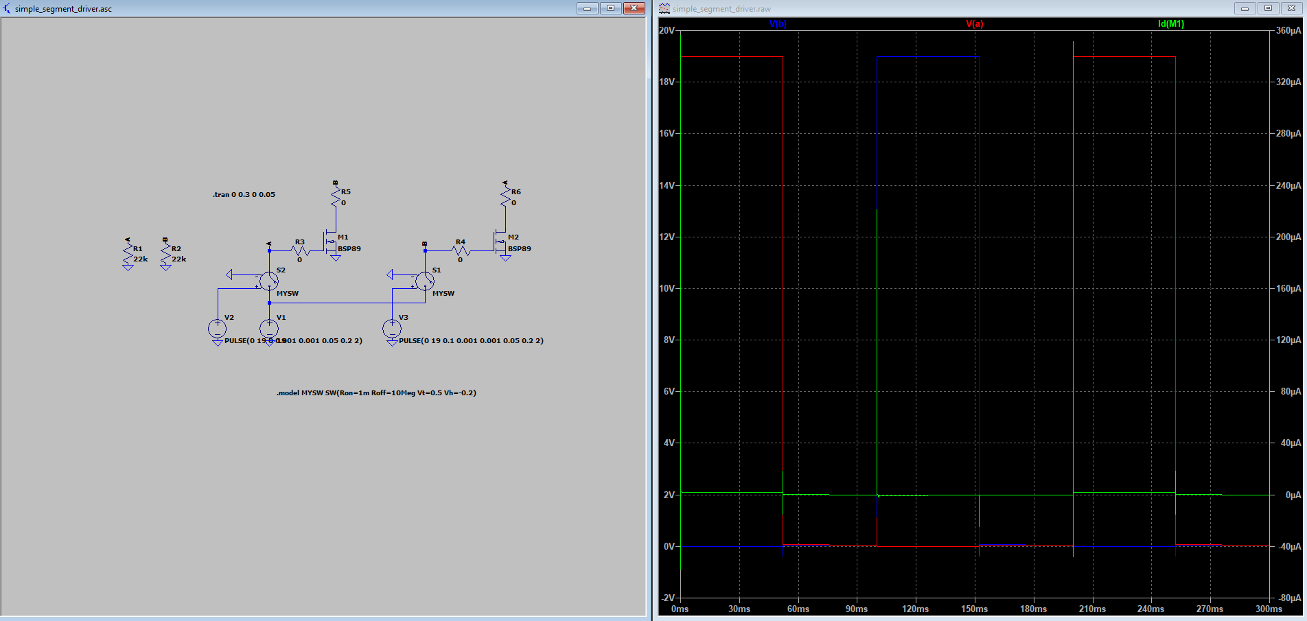
Everything works fine on LTSpice. But the real deal does not work.
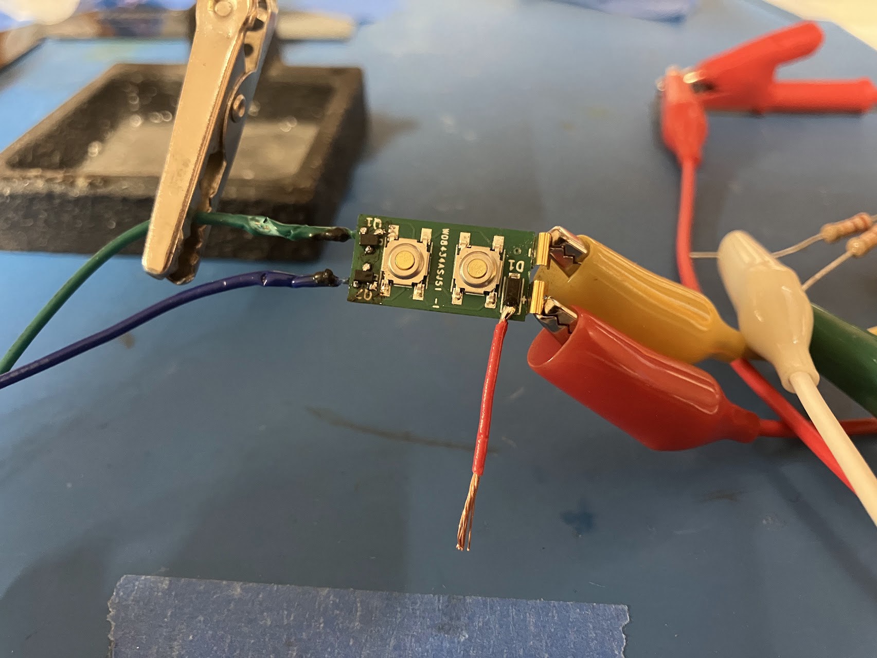
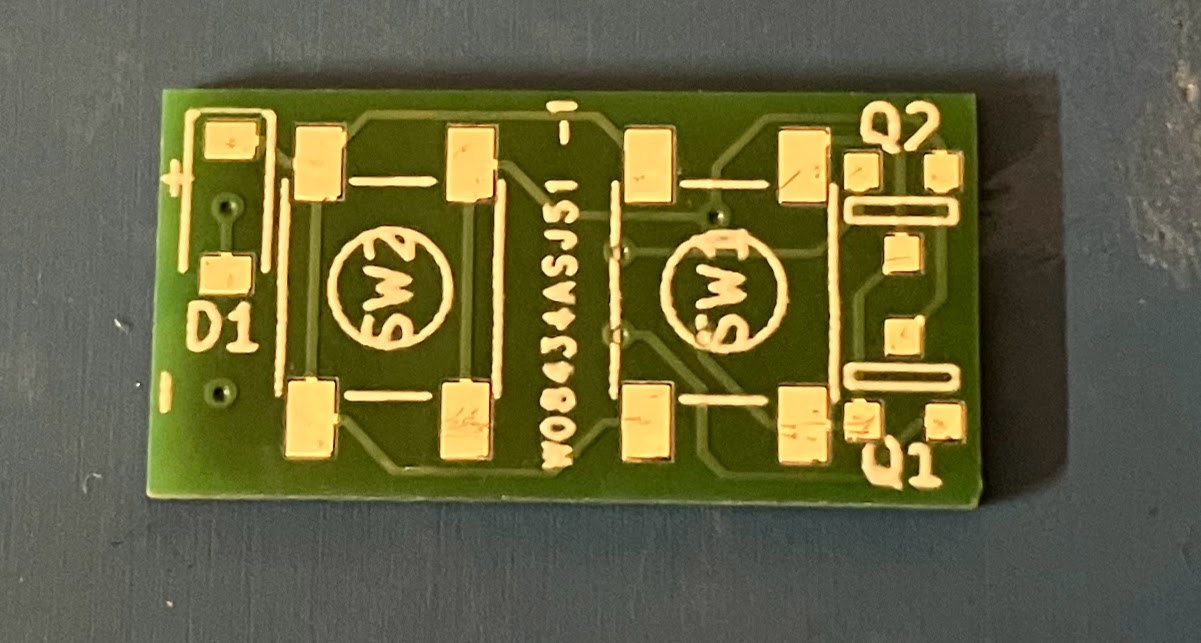
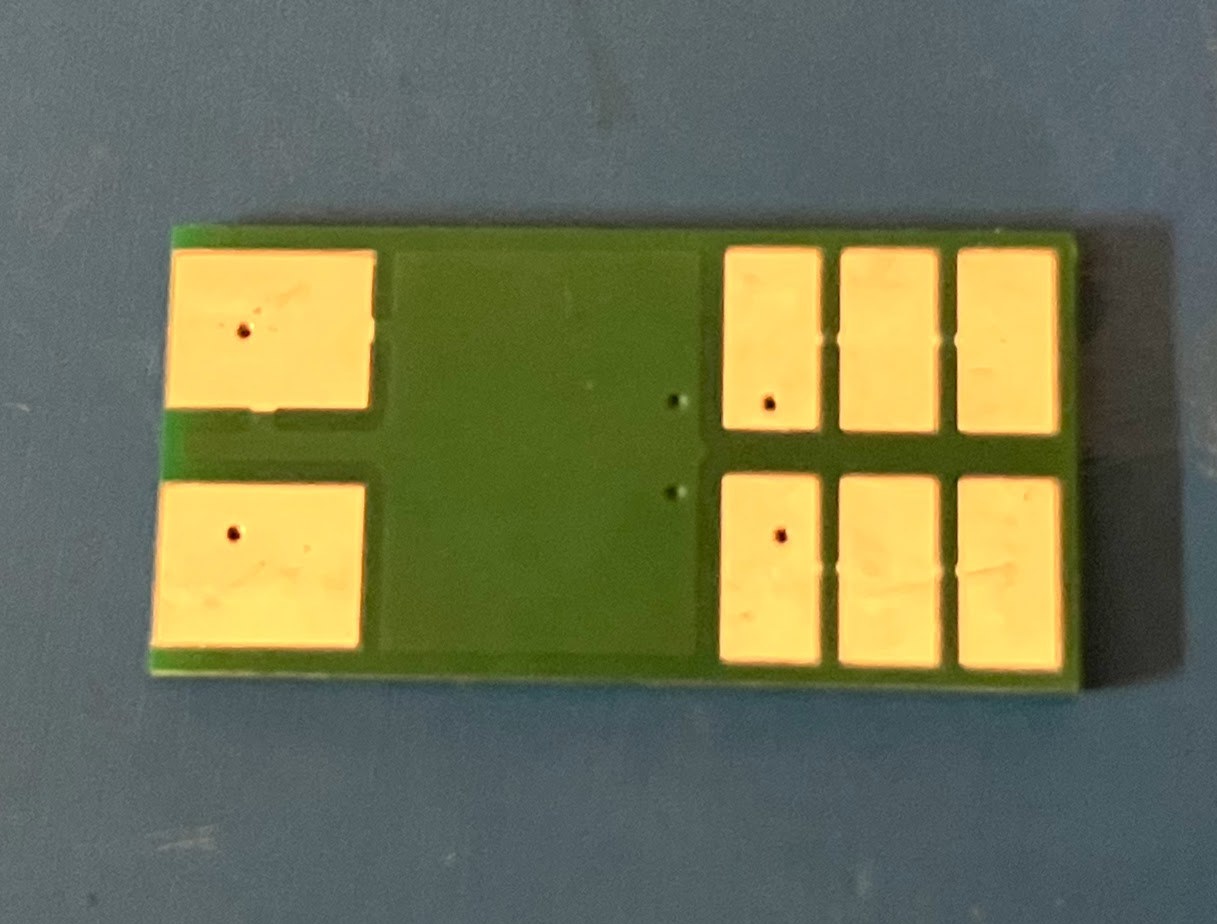
The circuit was implemented on a PCB. I built a batch of four boards and reflowed them. No malformed/shorted traces on the PCB as verified with Ohmmeter. Very simple circuit overall.
Test Conditions
Let VBAT = 25V, without any load attached to A,B:
When SW1 is Closed, VA->GND = 13.5V, VB->GND = 0.01V, I=7mA ->When current limiting diode is bypassed with +25V to +BATT, Q2 shorts to ground and smokes. Nothing happens to Q1.
When SW2 is Closed, VA->GND = 0.01V, VB->GND = 24.6V, I=2mA ->When current limiting diode is bypassed with +25V to +BATT, Q1 still conducts about 2mA, nothing happens to Q2.
When SW1 and SW2 are open, RA->GND = 0.8Meg, RB->GND = 0.8Meg. VA->GND = 0.3V, VB->GND = 0.3V.
Discussion
Seems to me like the MOSFETs are conducting electricity, even when the Gate voltage is clearly below Vgsth. They're conducting between 2 - 7 mA of current as measured by the power supply. R1 and R2 only contribute about 1.2 mA of draw. I have tested this circuit with R1 and R2 removed as well, with the same effect.
This same behavior has happened on multiple boards - not a single one works. I have switched out MOSFETs at least four times, even replacing them with MOSFETs from a different manufacturer, and the same thing keeps happening. The G,S and D are in the correct orientation.
The MOSFET should be able to handle everything. At no point do we ever exceed Vgs of +-30V. The resistors help discharge any residual capacitance in the system, so that we get lower Current spikes when the switches are engaged. According to the LTSpice model, we never exceed 1mA through either MOSFET when a switching event occurs. And the switching event is on the order of tens of uS.
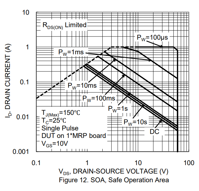 DMN67D8LW Datasheet Page 4 Figure 12, https://www.diodes.com/assets/Datasheets/DMN67D8LW.pdf
Does somebody else see something I am missing here? Or do I just have a bad batch of MOSFETs?
[EDIT 4-25-2024]
Wow, Electronics Stack Exchange is pretty helpful! Didn't think there would be so many responses.
By the way, thank you @Vicatcu for your CircuitLab Simulation. In the DC steady state simulation, everything worked great. Now the question remains, why isn't the real deal working?
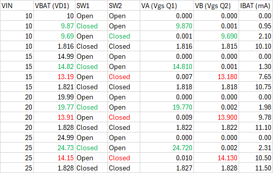
Nevertheless, there's a lot of data here to go over. Basically the problems are more noticeable when VBAT goes above 13V.
All voltages are measured relative to system ground. @Voltage Spike, We can be assured that VA = Vgs Q1, and VB = Vgs Q2 due to the electrical connection through the PCB. So long as the solder joints are good, and the amperage is low, the ground is common for all the components. Just to make sure, I did measure the gate pins directly, and they are equal to the corresponding A and B pads. And thanks for the pinout reminder - this I have gone over many times just to make sure.
I have built fresh boards from the ground up six times with brand new components, and I keep getting the same results. I have done both Reflow and Hand Soldering in different instances. I have used a proper Flux, an ESD Mat, insulating gloves, the whole nine yards. I track Reflow temperatures and profiles in my oven with three thermocouples, two on plate and one in air, plus I use distributed Thermal Stickers to make sure the temperature never exceeds 260 deg C. I recognize Mosfets are particularly sensitive to temperature, ESD, voltage and even amperage. @Jens, I added 33 kOhm chip resistors to the PCB directly across the MOSFET leads. I double checked joint quality with an inspection magnifying lens.
Take a look at this table of measurements.
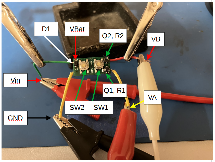
The voltages and amperages are measured with a Fluke 179. Everything was soldered down with quality connections, and the power supply clips are firmly clamped onto the feed wires. The output clips are firmly clamped to the multimeter. The results are fairly consistent among each of the boards.
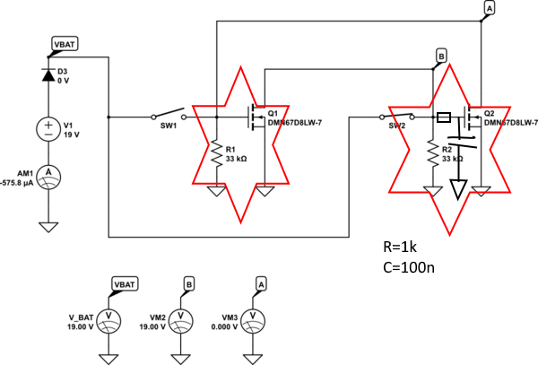
Here is the test circuit wiring diagram:
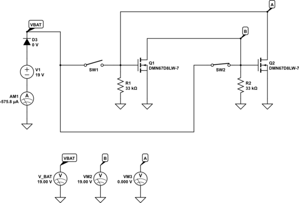
So why is it that Q2 conducts so much more than Q1? Why is this happening on every single board I checked? Why 13V?
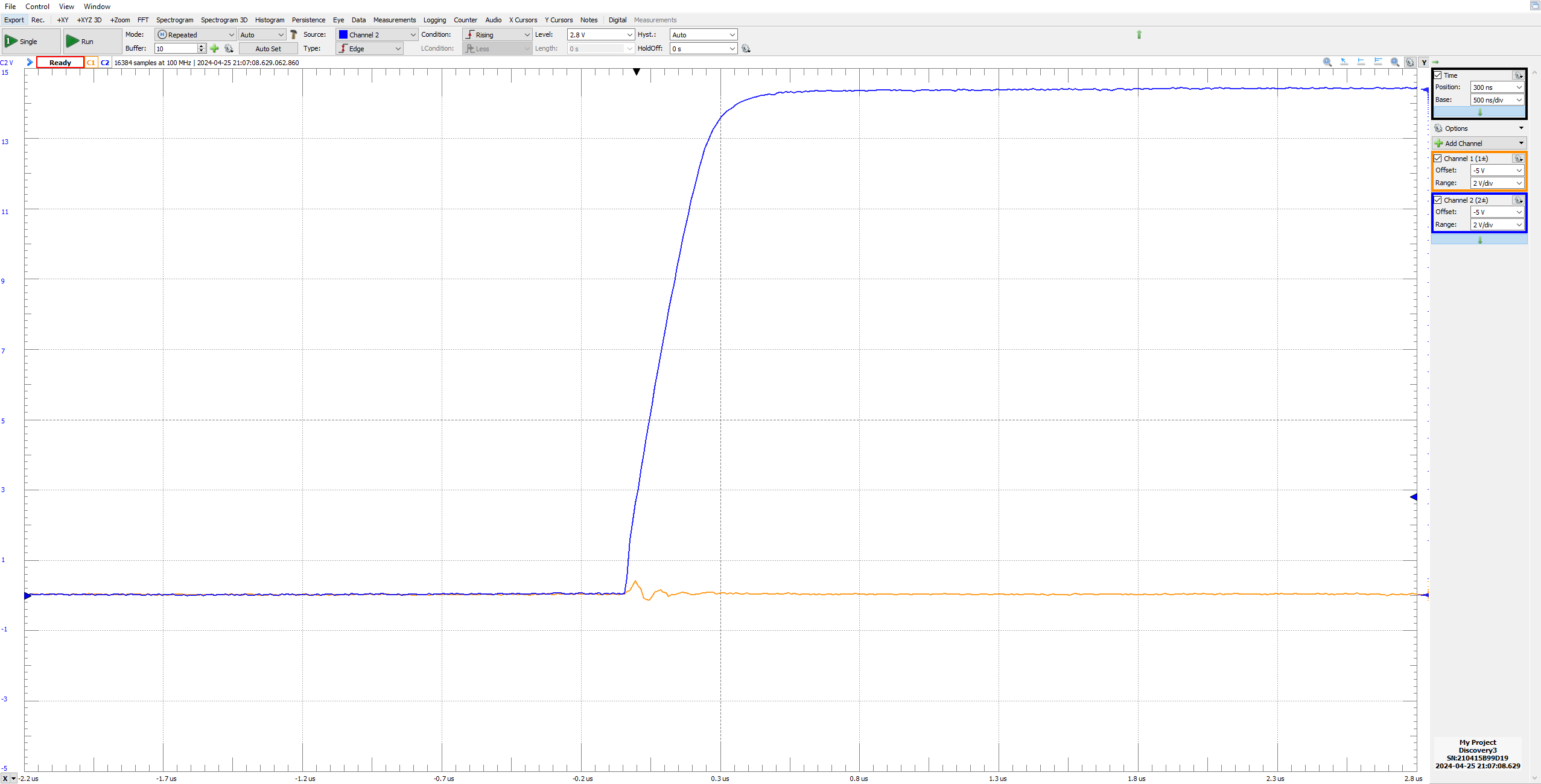
Captured on Digilent Analog Discovery 3. Signal 1 is VA, Signal 2 is VB.
Switch 1 closing, rising capture
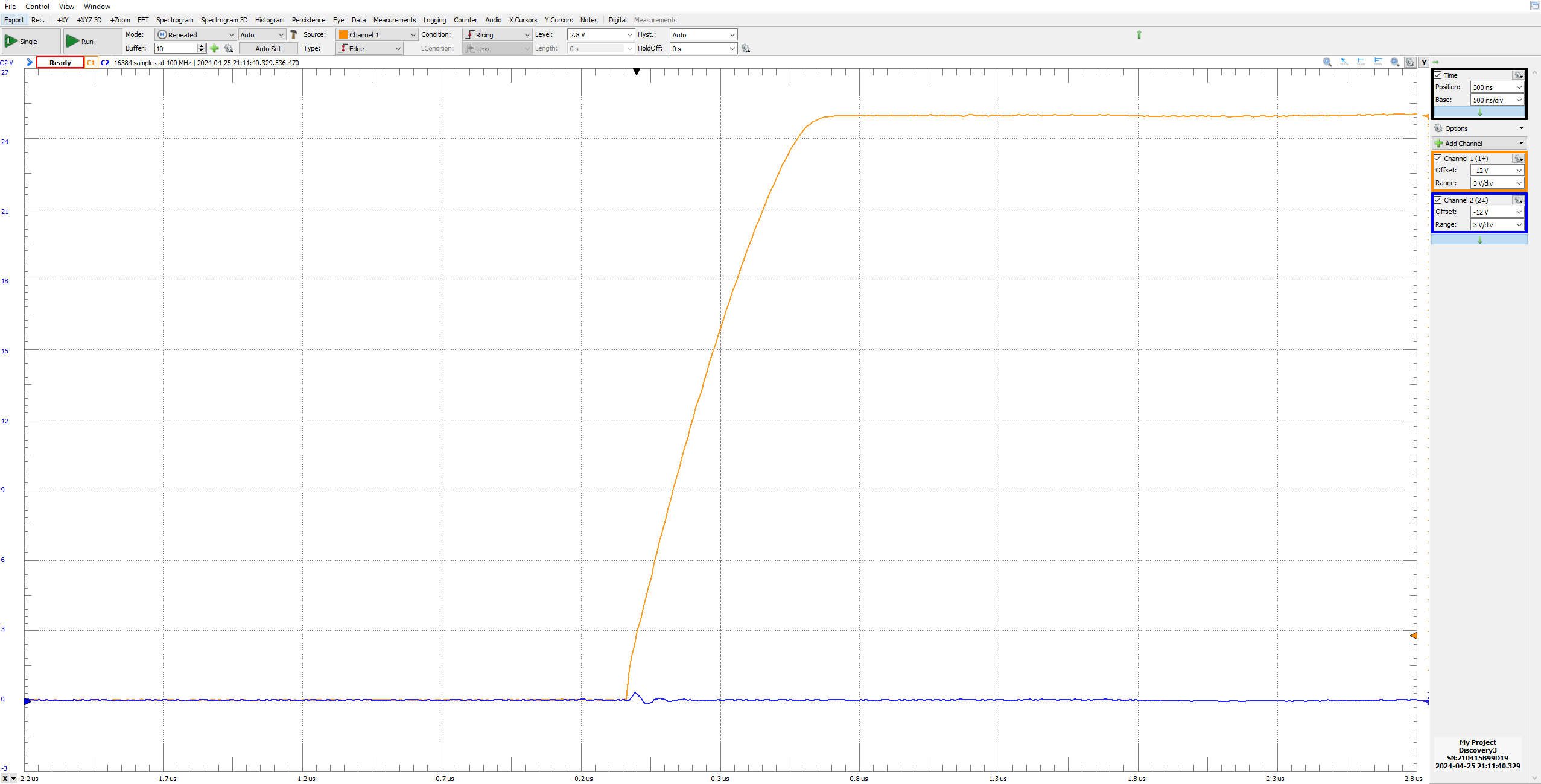 Switch 1 opening, falling capture
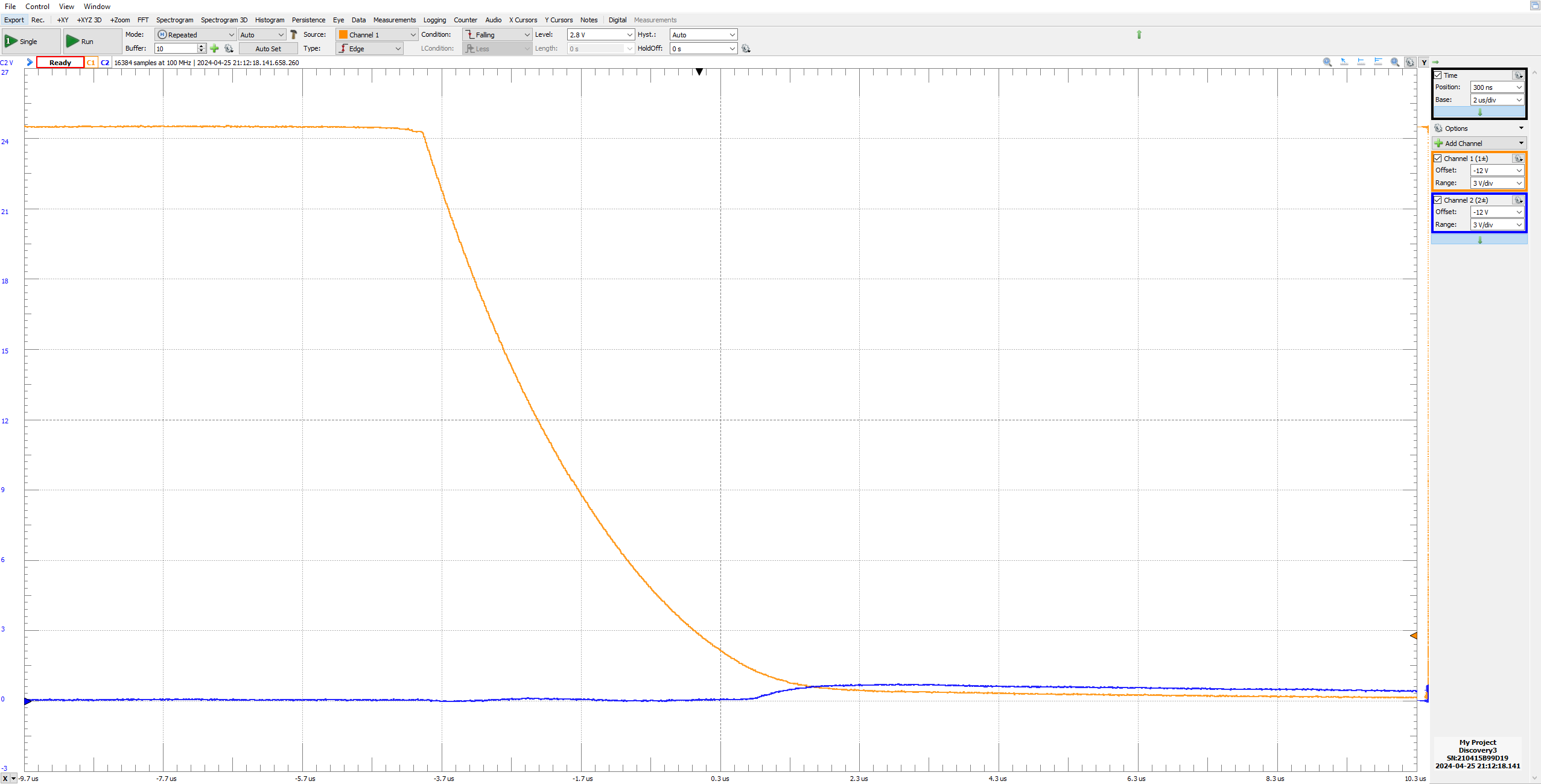 Switch 2 closing, rising capture
 Switch 2 opening, falling capture
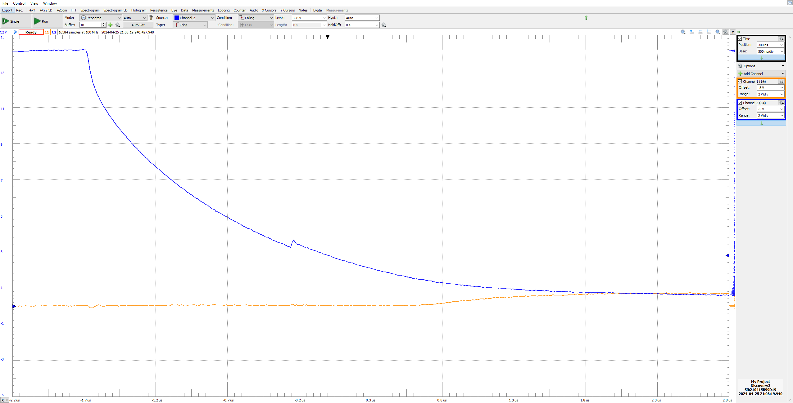
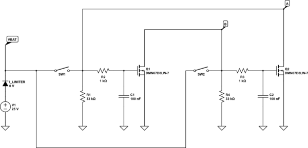
The oscilloscope maxes out at about 100 MHz, and the signal appears to be clean as a whistle. Maybe the gate is oscillating at super high frequency? Which may be keeping the gate partially open? I can't imagine how the circuit could maintain such a condition for very long. But we will add the RC filter to the gates next.
SOLUTION
Solution was to add an RC Filter as suggested below. WOW!

