1
\$\begingroup\$

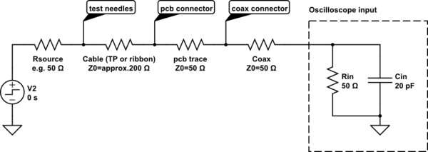
I am trying to design a circuit to transmit various digital high frequency signals over cables, connectors and pcb to an oscilloscope. The simplified circuit looks like this:

schematic

simulate this circuit – Schematic created using CircuitLab

I want to get minimum distortion of the signal with only resistors for impedance matching, but i don't really know how to determine the values and positions of these matching resistors. In my experiments i got the best results in following configuration:

schematic

simulate this circuit

Could someone explain what the correct way to get a solution for this problem is? And why the signal looked good in the given configuration? Also, what effects do the connectors (test needles, pcb connector) have on the impedance matching? Thanks!

EDIT: I want to measure the frequency of several different DuT's. The signal source could be for example: a microcontroller I/O, a digital clock IC or an oscillator. The main factors i want to measure is the amplitude and frequency of the signal. I "probe" the DuT with test needles and lead the signal via a ribbon cable or twisted pair cable to a pcb which on the other end has a coax connector. Then an oscilloscope is connected via a coax cable. The lengths in this system vary between 10 cm and 30 cm. The frequencys of interest are 10 to 100 MHz square wave and sine wave.

\$\endgroup\$
4
  • \$\begingroup\$ What's the rise time of your signal? What's connected to the test point and connectors? Describe the complete system or it's hard to give specific answers. \$\endgroup\$ Commented May 26 at 15:58
  • \$\begingroup\$ What are the (physical or electrical) lengths of the various elements? Are you sure the cable is 200 ohms? That's quite high. \$\endgroup\$ Commented May 26 at 16:13
  • \$\begingroup\$ @user1850479 The rise time is approx. 5ns. The source of the signal is not determined because there are several different DuT's. I will edit the question with a few additions. \$\endgroup\$
    – Robert
    Commented May 26 at 18:50
  • \$\begingroup\$ @TimWilliams The physical lengths lie in between 10 cm to 30 cm. I have already measured that there are transmission line effects present when measuring digital signals.. I have not measured the 200 Ohms yet. This was just an approximation for a higher value than the 50 Ohm impedance of the rest of the system. \$\endgroup\$
    – Robert
    Commented May 26 at 19:01

3 Answers 3

1
\$\begingroup\$

I assume that you are only worried about wave shape and not loss. You have a 50 ohm source and most transmission lines are 50 ohms, so your only issue is how to match the high impedance line. It is possible to do this using only resistors, and it will be broadband, but lossy. I started to derive the equations but was lazy and decided to google the result:

from: https://www.qsl.net/va3iul/Impedance_Matching/Impedance_Matching.pdf

enter image description here

You need two of these, one to go from 50 ohms to 200ohms, and another to go back. Also, as is clear from the formula for \$R_2\$, this configuration works for \$R_s > R_L\$ so this is the one for the RH end of the 200 ohm line. The other is the mirror image.

So calculate R1 and R2 from above using Rs = 200, RL = 50, and then use the following to make your 200 ohm line appear to be a lossy 50 ohm line.

enter image description here

If you have problems, apply some circuit theory and check the equations given.

\$\endgroup\$
2
  • \$\begingroup\$ Thank you @Tesla23. I calculated R1 and R2 and soldered them into my wire. The signal shape is almost similar to the configuration in my question. Is there a way to achieve this matching without using a resistor in shunt at the source? I'm a little bit worried about loading the source too much. \$\endgroup\$
    – Robert
    Commented May 27 at 8:34
  • \$\begingroup\$ If your source is happy driving 200 ohms, then you can simply leave out the matching between the 200 ohm line and the source. \$\endgroup\$
    – Tesla23
    Commented May 27 at 10:29
0
\$\begingroup\$

In general, you can't achieve this, but may be able to in specific circumstances. What you are trying to achieve is distortion-free transmission of the source signal to the load -- i.e. no multiple pulses or other waveform modifications. This is equivalent to saying a flat frequency response and linear phase delay (== constant time delay).

Impedance matching (to avoid reflections) only applies to systems where there are distributed elements (i.e. not lumped elements) -- this basically means transmission lines (e.g. coax cables, stripline etc.) which generate a time delay in the transmission of the signal.

In your 2nd diagram, the junction between R2 (150 Ω) and the trace (50 Ω) will cause a discontinuity. The reflection here will then travel back to the 200 Ω cable and reflect again at the junction of R1 and the source (because there is also an impedance mismatch here).

If you put 150 Ω in series with the source (at the source) and removed R1, you would prevent this particular reflection.

The connectors etc. tend to add minor mismatches and perhaps additional lumped capacitance to the network.

\$\endgroup\$
3
  • \$\begingroup\$ I hope OP doesn't think that a transmission line can be modeled by a single series resistor. \$\endgroup\$
    – Fred
    Commented May 26 at 16:32
  • \$\begingroup\$ Thank you for your answer. I added the 150 Ohm resistor to match the 50 ohm to the 200 ohm cable. I read in an article that when i terminate the 50 ohm coax and 50 ohm trace with a 50 ohm input resistor at the oscilloscope, i can see the system as a 50 Ohm resistor to ground. Because of that i thought i add a little bit of resistance to match the characreristic impedance of the test needles + wire. Is this totally wrong? When i started this project i tried to add a single resistor (can't remember the value) right at the needles and the signal was way more distorted than with the setup above. \$\endgroup\$
    – Robert
    Commented May 26 at 19:08
  • \$\begingroup\$ If you remove R1, and add another 150 Ω in series with the source, the 200 Ω cable will be matched at each end. While there is a MM at the junction of R2 and the PCB, reflections (backwards) here will meet a matched node at the left side of the cable, and be properly terminated. \$\endgroup\$
    – jp314
    Commented May 26 at 23:57
0
\$\begingroup\$

This sounds like a prime application to apply DFT (Design For Test) principles.

The more basic elements of DFT are such steps as, adding testpoints for all nets, or at least those that need them; making sure they're accessible (size, spacing, one sided if possible, etc.), and so on; which I'm guessing are already in play. Then, we can consider higher-level steps.

For example:

  • Mind that your probe circuit will load the signal -- you're adding a stub, or at least a low-value resistor (all the line impedances and terminations), messing up the amplitude, and probably the edge too. Consider adding a buffer before the probe point.

  • Instead of probing a clock line directly, probe a resistor or divider off it. Make a low-Z probe (450Ω into 50Ω transmission line -- or adjust as needed for other line characteristics).

  • Consider your needs. Do you need to check clock frequency? Perhaps a large-value resistor, or very small capacitor, would suffice to tap off the signal. Amplitude? A rectifier could be added. GPIO, a test program could set it static high/low; the test apparatus could then test its Thevenin source impedance in both states (thus avoiding a dynamic e.g. risetime test).

  • Limit risetime at the source. Depending on MCU, edge rate might be quite modest to begin with. Smaller or older e.g. AVR, PIC, etc. will mostly be in the several-ns range; faster/newer and lower voltage (3.3V or below) e.g. STM32, etc. can be fractional ns. Perhaps add a filter to slow the edge (good practice in general; for signals this fast, it can matter even just for on-board signals, let alone cables or probing!).

  • You might avoid probing high-speed lines entirely (e.g. LVDS, PCIe, etc.). Consider an alternative method, like design verification for signal quality (read: assume production is consistent), or device- or driver-level diagnostics to interrogate link quality.

    To further this, you might employ alternative controls: tagging traces as impedance-controlled to the fab; checking samples from time to time; placing test traces on the PCB so you can measure its impedance more easily, without having to tap into the important traces/ports themselves (a dummy trace between two SMA connectors (normally DNP'd) for example); etc..

  • Consider improving signal quality of the test harness in general. Use multiple ground probes near a given high-speed signal (or signal pair). Terminate them into a PCB (use press-in or soldered pogos instead of pogos fixed in a plate), or at least collect grounds plus signal into a coax cable for better signal quality.

  • Use twisted pair, probably preferably with shield to nearby multiple grounds, to maintain nominal differential and common-mode impedances.

    Note that twisted pair for single-ended signals is rather mediocre; you're launching a common mode Vpk/2 down the cable, which "wants" to be balanced, and some of that CM radiates away, couples with other things, etc., and grounding both ends of one wire guarantees strong reflections in the common mode, which the diff mode acts as a low-k transformer coupling into. The reflections can be absorbed in ferrite bead(s), or a differential receiver can be used to better terminate the line end (i.e., in a balanced manner).

Most of these wiring tips assume freedom to wire it as needed. Limiting things strictly to a ribbon cable, for example, has obvious drawbacks, and it's up to you whether that will affect things. You can at least reduce the impedance: typical ribbon cable is around 120Ω differential, 100Ω single-ended (G-S-G). You can roughly construct lower impedances by paralleling: a G-S-G-S-G arrangement (all G's and S's in parallel each) is... I think a hair over 50Ω? (It's not exactly half, because the two lines see each other just a bit.)

Many of these tips also incur some added cost from board-level components. If a PCB can be added above the test pins, a nearby termination resistor, or divider, etc. can be placed there, at modest expense to signal quality (the ~3cm stub of a pogo pin shouldn't be a problem for any LVCMOS signal), but the tradeoff is supporting a much longer interconnect back to the switch array / interface board / instruments. So too, any buffering you might add.

You mention that line lengths up to 30cm (a bit over 1ns electrical length) are present, and rise times down to 5ns. This sounds perfectly fine without detailed impedance controls. But you also mention that transmission line effects are evident, which seems to contradict this. Whatever the case, some of the above tips should probe useful.
\$\endgroup\$

Your Answer

By clicking “Post Your Answer”, you agree to our terms of service and acknowledge you have read our privacy policy.

Not the answer you're looking for? Browse other questions tagged or ask your own question.