1
\$\begingroup\$

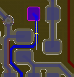
I'm designing a board that (among other things) elevate 3V3-I2C signals to 5V. The picture below shows one of the 2 BSS138 used for this task. It is connected to SDA-3V (topleft), SDA-5V (bottom) and 3V3 power (right), as shown.

two possible connections of BSS138

Due to the board configuration around this BSS138, I have to make the 3V3 track cross the BSS138.

I have two options: the first one (shown on the left) uses a narrowed track to go between BSS138 pads; all happens on the PCB front side. The second option (show on the right) uses two vias to make the connection through a track on the PCB back side.

Note that the full board has a ground plane on back side (not represented here), and thus the second option's track tears through this ground plane.

Could you provide some insight about which option is the better, and why?

\$\endgroup\$
2
  • \$\begingroup\$ How much current goes through those tracks? They look wider than necessary for any currents that would be reasonable for a BSS138. \$\endgroup\$
    – Hearth
    Commented Jun 3 at 15:43
  • \$\begingroup\$ Yes, they probably are. I tend to always use wide tracks unless something is telling me not to, but after a while, I forget they are too wide and that I can make them narrower without any drawback. Here the 3V3 track has 20mA max going through it. \$\endgroup\$
    – Silverspur
    Commented Jun 6 at 10:20

2 Answers 2

3
\$\begingroup\$

Two vias adds a few nanohenries of inductance to the trace vs a straight trace. If your application is in the 100MHz+ range of frequency, then you may want to see if adding these will affect your circuit. If under 100MHz it's likely that two vias will not make a difference.

You can calculate the added parasitics with a via inductance calculator

\$\endgroup\$
1
  • 1
    \$\begingroup\$ @TimWilliams Sorry, haven't woke up yet... \$\endgroup\$
    – Voltage Spike
    Commented Jun 3 at 16:01
1
\$\begingroup\$

Traces under SOT-23 are fine at standard design rules and IPC pad dimensions.

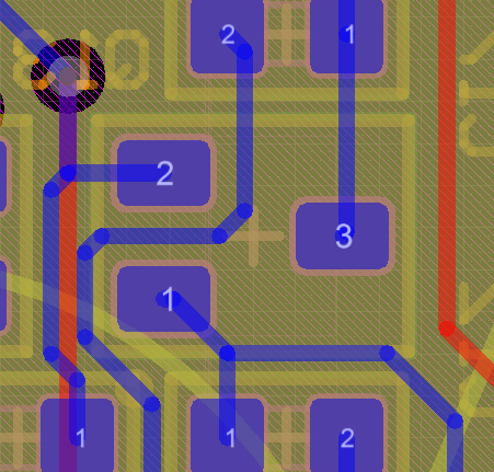
Showing clearances:

enter image description here

Pad (column) gap is 1.3mm, trace width and space are 10 mil.

enter image description here

Better view of the footprint and traces (top view bottom component so pin numbers are mirrored).

It seems your library components have ridiculously low pad gap / large heel dimension, which is questionable even just because it's putting solder paste underneath the component body (even at LMC), which doesn't make much sense.

\$\endgroup\$

Your Answer

By clicking “Post Your Answer”, you agree to our terms of service and acknowledge you have read our privacy policy.

Not the answer you're looking for? Browse other questions tagged or ask your own question.