2
\$\begingroup\$

I have to make an ADC conversion with an ATXmega MCU, in an air quality application.

The input is a voltage divider between a voltage reference. The sensing resistor vary in relation to a gas concentration. I read the voltage between a load resistor and ground. Since the conversion is not high precision (12 bit) we don't want to wast any bit. The sensing resistor can reach the max value of 60 k: in this case the V on the Load Resistor will be at minimum.

The solution we found is to subtract this minimum voltage from the Vin with an op amp.

And now the questions: The voltage divider interact with the resistors of the diff op amp circuit (https://en.wikipedia.org/wiki/Differential_amplifier)?

Will it be useful to place a unity gain buffer on between the Vref_min and the negative input pin of the op amp?

Is this idea is achievable with a normal low noise op amp like this?

http://it.farnell.com/texas-instruments/tl072ip/ic-op-amp-jfet-pdip8/dp/1459704 ?
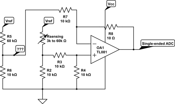
schematic

simulate this circuit – Schematic created using CircuitLab

Here the schematic. I have to put an unity gain buffer instead of "???" node?

Is the circuit ok?

\$\endgroup\$
4
  • \$\begingroup\$ Can you include a circuit diagram (edit your question, then hit Ctrl-M and draw one) and a link to the datasheet of the sensor? \$\endgroup\$
    – jippie
    Commented Jun 5, 2013 at 10:49
  • \$\begingroup\$ By adding a unity gain (buffer) amplifier you will get over the problem of source resistance, especially if the resistance varies. The tl072 is a good general purpose op amp but you might consider something with a bit lower noise such as an LT1012 or similar. \$\endgroup\$ Commented Jun 5, 2013 at 11:35
  • \$\begingroup\$ With your resistor to ground, what is the minimum voltage you get (sensor @ 60kohm) and what is the maximum voltage you expect (sensor @ minimum resistance)? \$\endgroup\$
    – Andy aka
    Commented Jun 5, 2013 at 11:40
  • \$\begingroup\$ @Andyaka it depends on Vref and Rload. With a Vref of 2.048V and a 10k Rload The voltage on Rl varies from 0.293V to 1.575. If i subtract 0.293V with a no-gain differentiator like in the schematic the range will be 0 - 1.282V, and I can use all the 12bit of the ADC conversion. \$\endgroup\$
    – Mark
    Commented Jun 5, 2013 at 12:55

3 Answers 3

3
\$\begingroup\$

If you have a reference voltage of (say) 3V, the range your input will see is: -

  • 3V * 10k/13k = 2.307V (sensor at 3kohms)
  • 3V * 10k/70k = 0.428V (sensor at 60kohms)

If you used a 50uA current excitation and a grounded sensor, the range your input will see is: -

  • 50e-6 * 3k = 0.15V (sensor at 3kohms)
  • 50e-6 * 60k = 3.0V (sensor at 60kohms)

With a current excitation the percentage of your 3V reference range used is 95%. With voltage and resistor excitation you only get 63% of the range.

If your reference voltage is lower or higher, the above "range" statements are still true.

enter image description here

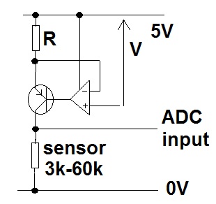
Here is an example. An ADC input is directly connected to the sensor. The sensor is fed with 50uA via the PNP transistor. The 50uA is measured across "R" and compared with "V" by the op-amp. The op-amp keeps the current through R at a value that generates a voltage "V" across it. Values could be R=10k and V=0.5V or R=20k and V=1V. Op-amp should be chosen that has close-to-either-rail IO performance like an AD8605 (used many times by me in this same configuration for strain gauge excitation).

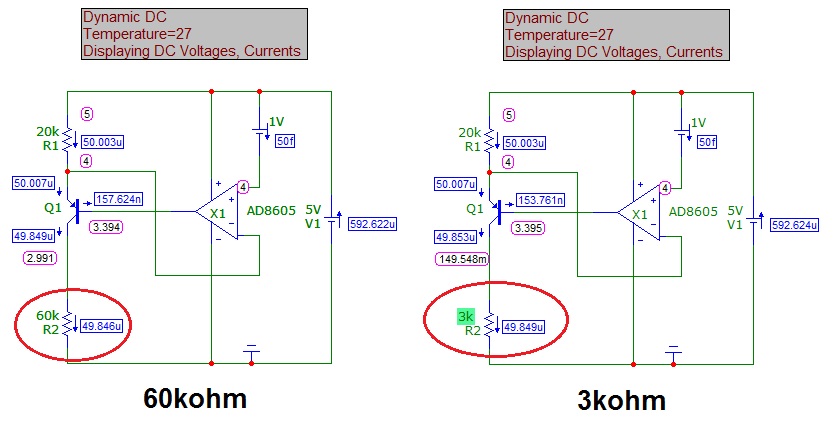
Here's a quick DC simulation for 60k and 3k loads: -

enter image description here

Transistor used is BC547C or BC847C for those with good eye-sight.

Note that due to small base currents in the transistor, the current isn't 50uA but 49.846uA with 60kohm load and 49.849uA when loaded at 3kohms. Note also the voltages across the sensor - 2.991V on 60k load and 149.5mV on 3k load.

\$\endgroup\$
24
  • \$\begingroup\$ The problem is that the internal reference of the ADC is 1V, so I need to concentrate the output of the op amp in the range [0-1V] or [0-2V] (the last with a 0.5 internal gain). I have no experience with current excitation.. \$\endgroup\$
    – Mark
    Commented Jun 5, 2013 at 13:04
  • 1
    \$\begingroup\$ @Mark - For current excitation think of a constant current source that produces a low level of current into the sensor resistor. As Andy indicated the other side of the sensor resistor is grounded. This scheme allows full use of the A/D input range because the excitation current can be set to that it produces the max A/D input when the sensor resistor is at its highest value. The current source wants to be biased from some voltage rail that is higher than the A/D input range so that the current source has enough compliance to deal with the changes in load on it. \$\endgroup\$ Commented Jun 5, 2013 at 13:13
  • \$\begingroup\$ @MichaelKaras I couldn't have put it better my self. \$\endgroup\$
    – Andy aka
    Commented Jun 5, 2013 at 13:19
  • \$\begingroup\$ Sounds good. I ask you another step. In your scheme I put a 20K resistor R and a V of 1. When Rsense is at maximum val = 60k the overall resistance is 80k, so the current is 12.5mA. i dont see the role of the op amp in this circuit. There must be a voltage difference between the two R pin, so the PNO is always excited. Or not? Thanks guys! \$\endgroup\$
    – Mark
    Commented Jun 5, 2013 at 13:34
  • \$\begingroup\$ @Mark you must have got this wired up incorrectly. The 1V needs to be referenced to the positive supply rail (5V). The currents drawn should be 50micro amps certainly not milli-amps. The op-amp is needed to stabilize the voltage across the resistor to exactly 1V an 1V divided by 20kohms is 50 micro amps. Are you simulating it? \$\endgroup\$
    – Andy aka
    Commented Jun 5, 2013 at 13:38
1
\$\begingroup\$

While this doesn't directly address your question, it does describe a problem you are going to run into in the near future.

Basically, the ATxmega ADCs are pretty much unusable when connected to the xmega's internal 1.0V reference. You get ~16 counts of noise no matter what you do.

The general consensus seems to be that if you want to use the ADxmega internal ADC, you really have to use an external reference. Ideally, you could use the entire 0-3.3V range, but the ADC only supports references up to Vcc - 0.6V, so 2.5V is probably the best idea.

I recently was working on a project that had some user-interface pots that were connected to the xmega ADCs. I indeed wound up having noise issues. I was able to solve them by massively oversampling (x4096 times!), but it still only gave me maybe 10 bits of usable resolution.
Now, my layout was really, really non-ideal (the UI stuff was added after I had sent the boards off to be fabbed, it was hung off what was supposed to be just a debugging port, and had wires everywhere and whatnot).

Atmel has supposedly "fixed" the ADC issues on parts with the "u" suffix (Such as ATxmega32A4U vs ATxmega32A4), but I have not had a change to work with the "U" parts.

\$\endgroup\$
4
  • \$\begingroup\$ Thanks a lot, I read on avrfreaks about this issues with the internal 1V refence. My idea is to test it, and find out if the ATXMega256A3BU has a fixed ADC internal reference. I think thaht if the conditioning circuit and the driver are well designed it will be possible to insert in a second time an external reference, changing resistors and a few lines of code. Do you agree with this plan? Have you experienced ADC voltage reading on a resistor? You used current excitation or voltage divider? \$\endgroup\$
    – Mark
    Commented Jun 6, 2013 at 7:20
  • \$\begingroup\$ @Mark - I was just taking ADC readings of a straight-up voltage divider, single-ended mode, with no external reference (I didn't have the pins!), so I can't really comment on the viability of other options first-hand. \$\endgroup\$ Commented Jun 6, 2013 at 8:42
  • \$\begingroup\$ If I were in your situation, I would add the PCB footprints for adding an inexpensive 2.5V reference on the PCB, and have some optional 0Ω resistor footprints so you can install it and connect it up if your plan for signal conditioning doesn't pan out. It's worth noting that the filtering on the analog input probably won't help much, as the noise is internal to the ADC. Your options are really just: 1. Use an external vRef, 2. Use the internal voltage divider off Vcc, and 3. Use the internal vRef, and decimate the hell out of it. \$\endgroup\$ Commented Jun 6, 2013 at 8:45
  • \$\begingroup\$ There are some really, really cheap voltage references out there. The LM336Z25 is $0.51 in single quantities on digikey. That, a resistor, and a cap would be all you need. \$\endgroup\$ Commented Jun 6, 2013 at 8:51
0
\$\begingroup\$

Yes, you can buffer the inputs to the differential amp, and there may be reasons to do so. However, an Instrumentation Amplifier like the AD620 is already pre-buffered and has easily adjustable gains. If You need single-sided rail-to-rail functionality (one power supply), there's the AD623.

\$\endgroup\$
1
  • \$\begingroup\$ The low cost is an important feature for this project. Obviously without killing performance. I proposed the TL072IP beacuse it has two channels and it's possible to use one channel for buffering the negative input and the other channel for the differential operation. And it cost 0,68€ vs the 5.14€ of the AD623. \$\endgroup\$
    – Mark
    Commented Jun 5, 2013 at 13:20

Your Answer

By clicking “Post Your Answer”, you agree to our terms of service and acknowledge you have read our privacy policy.

Not the answer you're looking for? Browse other questions tagged or ask your own question.