3
\$\begingroup\$

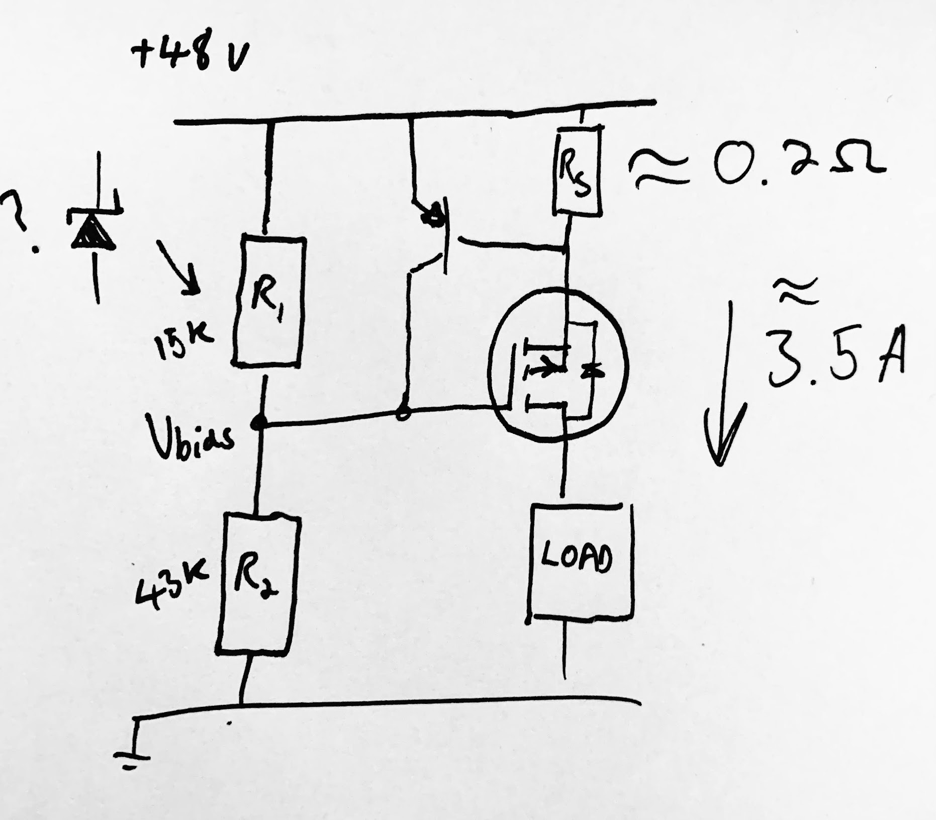
I started out experimenting with a very basic current limiter that begins to pinch off a pmos when about 0.7 V drops across a shunt

enter image description here

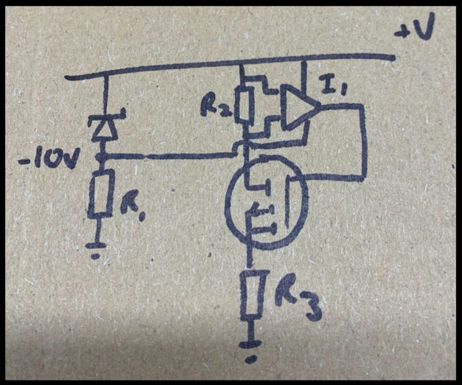
I then decided I wanted to be able to trim the current with a pot and have a bit more predictability, so moved to a design with a dedicated current sense amplifier. The following circuit basically functions on the breadboard, but the current limit is not a hard threshold. It varies with R1 and R3. The current sense amplifier is a MAx4080S with a gain of 60. I'm doing a bit of a hack where I use a ground reference off a zener, so when theres no current across the shunt, the output is zero (i.e. about -10 V) and as current flows through the shunt, the voltage drops and is amplified and pinches off the pmos. I'd like it to work more predictably if the source voltage sags or the load impedance changes. How could I go about improving this design?

Additional info: This circuit operates off a PWM drive signal (sometimes 10% driven in the range of a few kHz) from another circuit that is low-side switched. The regulation needs to kick in fast. The 48 V might sag down to 40 and the load impedance is unstable. I need to drive everything off the 48 V(ish) supply I have (hence choice of 4080)

enter image description here

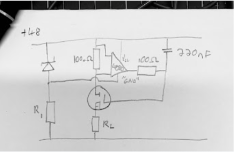
A scope across the load shows current oscillating at 83 kHz! Why (there is a 100 Ω resistor between the output of the amp and the gate)? Schematic 3 below removes the oscillations but the integrator wind up is huge (~500 µs)

enter image description here

\$\endgroup\$
4
  • \$\begingroup\$ Got a model number for that MOSFET? Your amplifier can't drive more than 500 pF. If you increase the 100 ohm resistor (not shown in your schematic) do the oscillations stop? \$\endgroup\$ Commented Jun 17 at 18:01
  • \$\begingroup\$ It will vary with R1 and R3 but, you didn't say how much. Where is the 100 ohm resistor in your schematic? \$\endgroup\$
    – Andy aka
    Commented Jun 17 at 18:22
  • \$\begingroup\$ 100 ohm between amp and gate. Oscillating stopped putting a 220 nF (was easiest to reach) cap between gate and positive rail.. works better but still seems naff using a zener as the ref for the diff amp. Just the first thing that came to mind \$\endgroup\$
    – learnvst
    Commented Jun 17 at 19:36
  • \$\begingroup\$ @learnvst This EESE answer provides methods for using datasheets and calculations to achieve a desired goal in predictable and thermally stable current control. It also exposes some limitations/boundaries, as well. No FET and no oscillation tendencies. But I've no idea what kind of accuracy (initial or long term) you require, if any, or how tight the precision must be, regardless. \$\endgroup\$ Commented Jun 17 at 23:17

4 Answers 4

3
\$\begingroup\$

The regulation needs to kick in fast. The 48 V might sag down to 40 and the load impedance is unstable

enter image description here

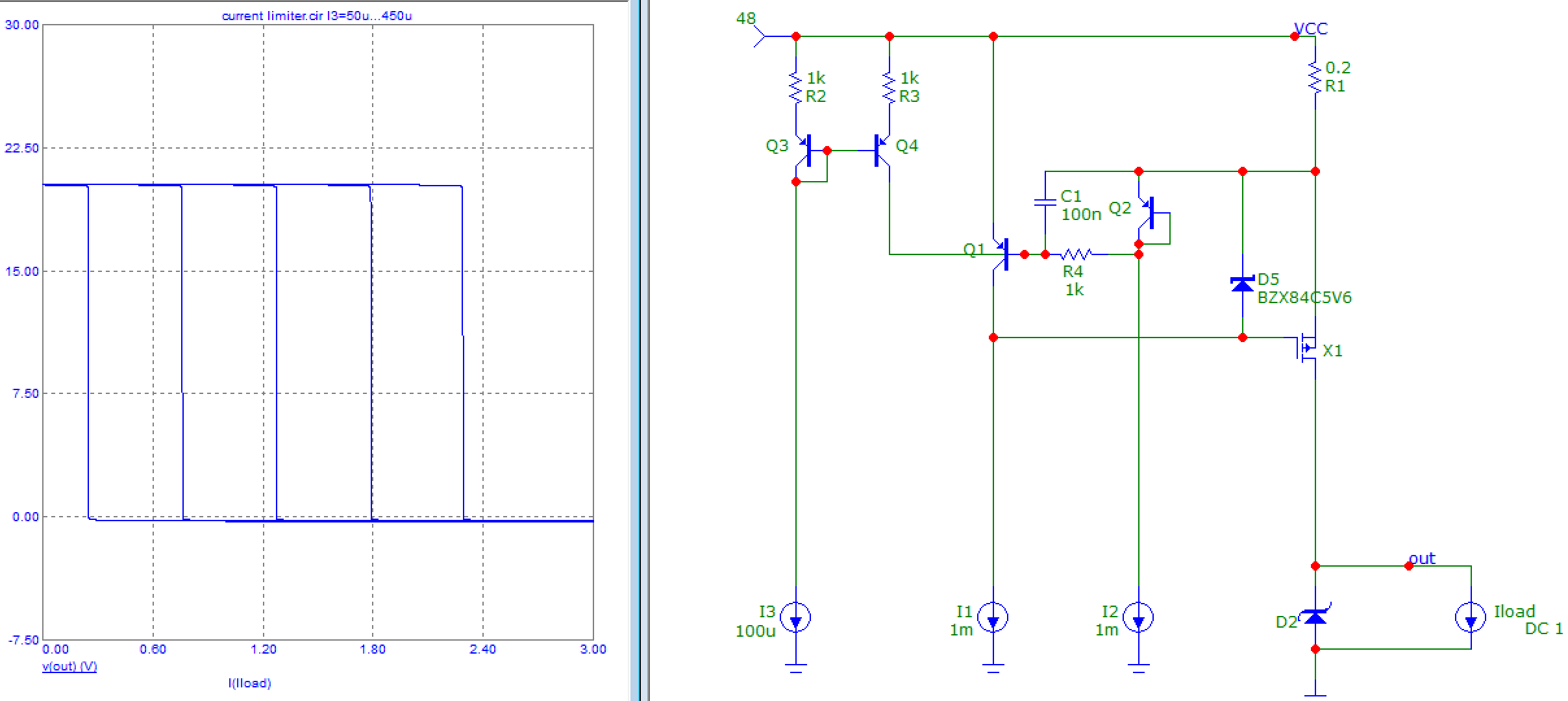
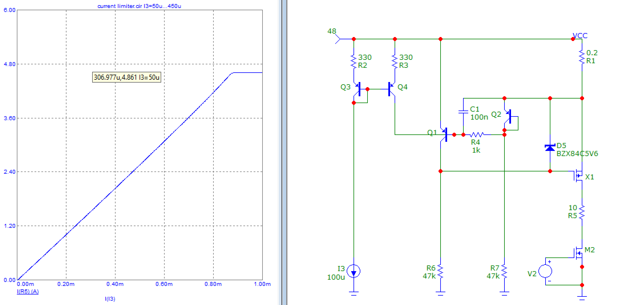
Q1 and Q2 should be a dual matched transistor like BCM857. These dual transistors have pretty close Vbe match if both run at the same operating point and at the same temperature. Q2 is wired as a diode with a constant current bias (I2) and creates a voltage drop that cancels Q1's Vbe. This makes a current limiter by pulling on the MOSFET gate, with the current limit set to zero instead of one Vbe across R1. Current mirror Q3,Q4 applies a current across R4 to add some threshold voltage back, which sets the current limit. Thus the control input is I3.

This has a bit higher offset and drift than an opamp, so it will be less accurate, but it is faster because the bandwidth of the error amp (Q1) is higher than what the usual current sense opamp offers. The MOSFET gate is current driven and compensation is provided by the MOSFET's gate capacitance and Miller effect.

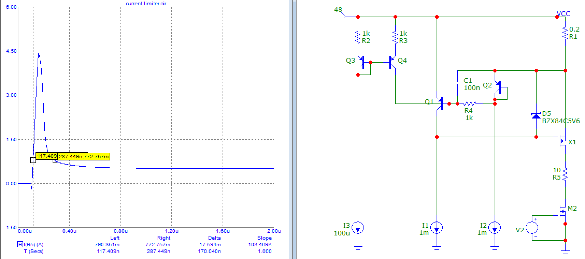
I added a low side switch and load resistor. The current limiter acts in about 170ns:

enter image description here

To suppress this overshoot, a solution would be to re-architect the circuit: instead of a low side switch and a high side current limiter that acts "after the fact", you could use a low side switched current source. Instead of overshoot, this will result in a delay to ramp up the current, which can be a better option.

On second thought, the current mirror resistors are too high at 1k, a lower value is better to avoid saturating Q4.

enter image description here

\$\endgroup\$
17
  • \$\begingroup\$ Hi @bobflux. Thanks so much! I have built this (just with discrete 2907 PNP for now). I'm using 47k resistors to ground to approximate I1 and I2. Trimming I3 with a pot and I get limiting with 1.1mA - 1.3mA, not the 100n you show. Why could this be? I guess I need to use some sort of precise sink here or any sag in Vcc will throw this out? What is C1 doing? Why the 5v6 zener? \$\endgroup\$
    – learnvst
    Commented Jun 19 at 13:51
  • \$\begingroup\$ Zener protects the FET gate against overvoltage: when below the current limit, Q1 is off, I1 pulls the FET gate to ground, so you'd get 48V Vgs, way too much. Zener voltage should be enough to get a good turn on of the FET but not more, as extra voltage on Vgs only serves to make Q1 have to remove more charge out of the gate, which makes the current limiter slower when it has to act. \$\endgroup\$
    – bobflux
    Commented Jun 19 at 13:58
  • \$\begingroup\$ C1 just makes it a little bit faster, to drive Q1's base with low impedance. It's an extra, not strictly necessary. I have no idea why you have to put so much current into I3, in fact with 1.1mA it should not work. I've simulated again: 47k resistors instead of I1 I2 is fine. R2 R3 would be better at 330 ohms to avoid saturation on Q4. \$\endgroup\$
    – bobflux
    Commented Jun 19 at 15:30
  • \$\begingroup\$ Thanks bob. It limits and it does so pretty quickly. There is a peculiarity in that there is the initial overshoot on the timescale you describe, but on the bench there is a subsequent dip and then recovery. Not like ringing, rather spike, total shutdown, then up to a limit. I'll see what happens with 330Rs on the mirror \$\endgroup\$
    – learnvst
    Commented Jun 19 at 15:40
  • 1
    \$\begingroup\$ I get the behavior you describe (peak, shutdown, ramp) in simulation if C1 is omitted. It is due to Q1 not having enough base current. C1 provides the base current spike required for Q1 to discharge the FET gate quickly. \$\endgroup\$
    – bobflux
    Commented Jun 19 at 16:07
2
\$\begingroup\$

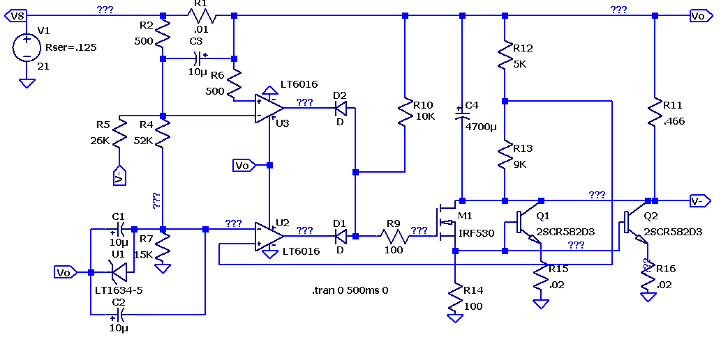
Perhaps this might help. I have a working high current 12-volt power supply. I have used the design in roughly 50 DC power supplies with voltage and current limiters replaced with this LDO regulator. It looks a little busy initially, but isolating the circuits is straightforward. The current limiter consists of R1, R2, R4, and U3. The output of U3 is diode OR’ed with U2, the voltage regulator, to control the output of M1.

The design allows for exact voltage and current control using a precision voltage reference created by U1, R7, C1, and C2. The output of U1 provides the reference for both the Current and Voltage regulators.

To control the current, replace R2 with an appropriate-sized resistor or potentiometer. For example, 100 to 500 Ohms will produce 5 to 30 amps output. Ignore R5, which is a Voltage Foldback resistor.

If you eliminate U2, D1, R12, and R13 (the voltage regulator), you have a precision current supply. The Op Amp must have a high CMRR and PSRR to avoid the high-side current limit/monitoring.

Hope that helps

12-volt High Current Power Supply Battery Charger

\$\endgroup\$
2
  • \$\begingroup\$ Many thanks for the input. The LT601X range of op amps look interesting for this sort of application \$\endgroup\$
    – learnvst
    Commented Jun 19 at 23:38
  • \$\begingroup\$ LT601X is explicitly made for the application. \$\endgroup\$
    – Dereck
    Commented Jun 20 at 14:41
1
\$\begingroup\$

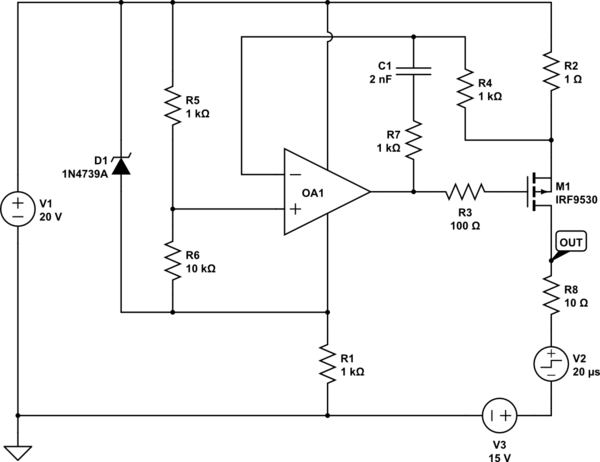
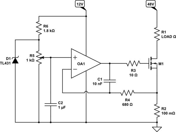
You need an op-amp and reference voltage, not a current amplifier. The amplifier is fixed-gain, which sets output current in terms of Vgs(th), which is poorly defined. In both cases, you likely need compensation to avoid oscillation, as the MOSFET has high capacitance

schematic

simulate this circuit – Schematic created using CircuitLab

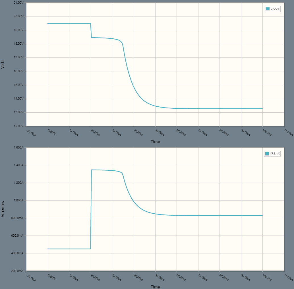
Note you'll still have "integrator windup", i.e. normally while the output is saturated, the amp is saturated to +V, and it will take some time to slew up to Vgs(th) and begin regulating. This manifests as a "diode reverse recovery" sort of response, the current peaking initially before settling down, the peak amplitude varying with rate (dI/dt):

enter image description here

With proper tuning (choice of op-amp, MOSFET and compensation components C1, R4, R7) this can be reduced to a few µs easily enough.

\$\endgroup\$
2
  • \$\begingroup\$ Many thanks for the input, Tim. Between putting out fire, I also see (far worse) integrator windup in my own schematic 3. If I understand this your circuit here is a variant of the one posted by user MOSFET but driving the inverting input directly from the VR2. Do I understand this correctly in that R5 and R6 form a voltage divider that sets a reference that can be trimmed to adjust current? \$\endgroup\$
    – learnvst
    Commented Jun 18 at 10:00
  • \$\begingroup\$ Correct. They're doing the same things, in different places. I chose to elaborate on your original, correcting it to a familiar form (op-amp current source, high side referenced). MOSFET's uses a current sense amp (potentially allowing lower saturation voltage) and a level shifter so the op-amp and also reference input voltage (R7 divider) are ground referred (low side). This requires a level shifter (Q1) to drive the MOSFET. \$\endgroup\$ Commented Jun 18 at 13:32
1
\$\begingroup\$

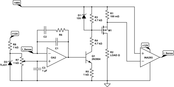
Your first circuit doesn't work the way you want because you lack a precision reference - Vbe is not a precision voltage reference. Your second circuit has the same problem as the first, but this time, the amplifier is unstable because you have no compensation for the capacitive load presented by the MOSFET gate. Here's how I would do the circuit that will do what you want:

schematic

simulate this circuit – Schematic created using CircuitLab

This is a High-current, constant-current source. But it will function as a current limiter.

There are simpler solutions available if you are doing low-side sensing. Even simpler if you're load was only a few hundred mA. The issue is detecting a lot of current while minimizing heat in the shunt resistor. INA293 and R1 could be replaced with a hall-effect current sensor. The exact details of the design will depend on your application requirements.

Edit: updated schematic per @TimWilliams observation.

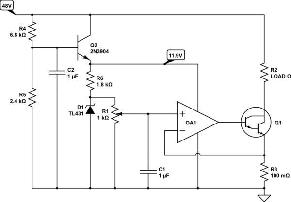
Per comments, here's the simpler low-side version:

schematic

simulate this circuit

Or with the Darlington:

schematic

simulate this circuit

This one also has an added unregulated power supply to bring down the 48V. It could be used in all three circuits I posted. There's a lot of flexibility here so the parts aren't critical and performance can be easily tailored.

\$\endgroup\$
13
  • \$\begingroup\$ Thanks for the help. I'm trying to unpack this schematic. On the right is basically what I have in my second schematic, but the shunt amp now drives an opamp stage. Down the middle you have an NPN pulling the gate of the pfet to gnd via 4k7. So Q1 not conducting has VGs=0, and Q1 wide open has VGs=-15 (am working this out as I type). Ok cool - that gets rid of janky GND via zener . So why can't we drive Q1 with the output of the current sense amp through a voltage divider (nasty vbe reference?)? Low-side solution is also something I'd be interested in. \$\endgroup\$
    – learnvst
    Commented Jun 18 at 9:25
  • 1
    \$\begingroup\$ Another thought . . . can we not just swap the OA and Q1 out for a TL431 with the reference driven from the output of the current sense amplifier? \$\endgroup\$
    – learnvst
    Commented Jun 18 at 12:53
  • 1
    \$\begingroup\$ A note, Q1 should have emitter resistance to degenerate it, giving stable gain; the hard-grounded emitter gives exponential gain, causing the loop time constant to vary with condition. This also limits current (assuming OA2 +V is specified) allowing R5, R4 and potentially D1 to be removed (you might keep D1 just in case, but do add a ferrite bead to it to avoid creating a tuned-gate oscillator). \$\endgroup\$ Commented Jun 18 at 13:36
  • 1
    \$\begingroup\$ @learnvst The opamp is a compensator with DC gain as high as the open-loop gain of the amplifier. C1, C2, And R6 are the compensating elements to adjust poles and zeros based on the poles and zeros presented by all other elements in the FB loop. You may not need all those comp elements based on loop response and desired performance (high-speed vs overshoot tolerance). \$\endgroup\$
    – MOSFET
    Commented Jun 18 at 17:15
  • 1
    \$\begingroup\$ @learnvst I made it up - It, too, is also compensation. It works with C1 to set the dominant pole. R3 decouples some of cap load from the amplifier. 680ohm is a good first-guess that will get you going pretty much no matter what. higher value gets you more stability at the expense of a slower response. Keep going lower until you get overshoot that you can't tolerate. May have to tweak C1. I made that up too. I'm not at the bench designing your actual circuit. lol \$\endgroup\$
    – MOSFET
    Commented Jun 18 at 17:27

Not the answer you're looking for? Browse other questions tagged or ask your own question.