0
\$\begingroup\$

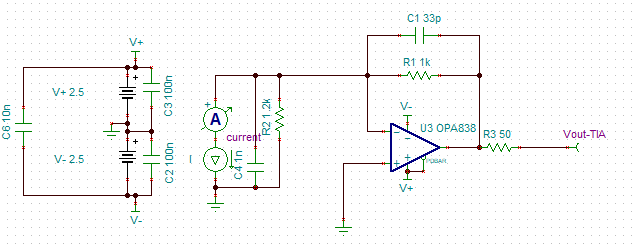
I have designed a transimpedance amplifier as follows:

Transimpedance amplifier schematic

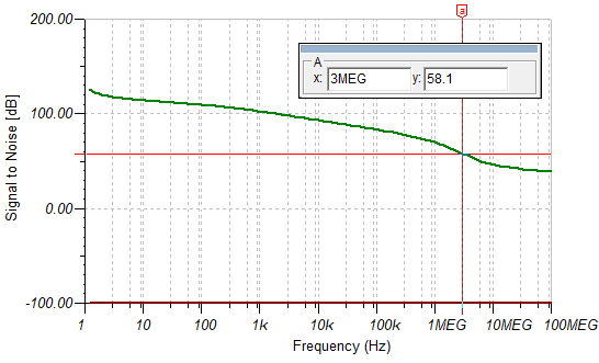
Based on the simulation, I should get around 58 dB for SNR @3MHz:

Simulation response graph

But what I achieved in my experimental results is as follows:

  • Supply voltage +/-1.5 V

  • Power consumption 900 µA (datasheet=950 µA)

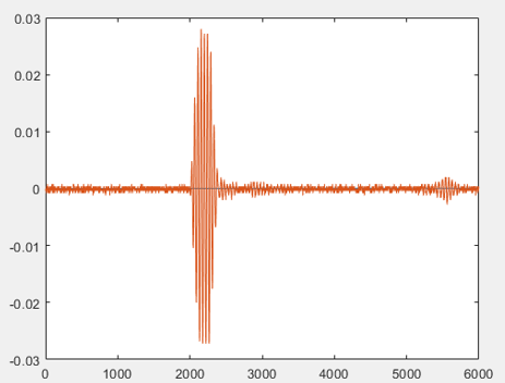
Output signal:

Output signal

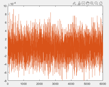
Noise:

Noise

Calculations:

-〖Signal〗_RMS= 3.8 mV

-〖Noise〗_RMS= 0.25 mv

-SNR (MATLAB)= 23.4 dB (I used snr() function in MATLAB to calculate the SNR)

-SNR (Calculated)= 20log(〖Signal〗_RMS/ 〖Noise〗_RMS)= 23.6 dB (calculation by hand)

Circuit design:

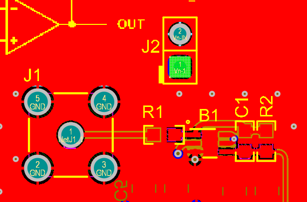
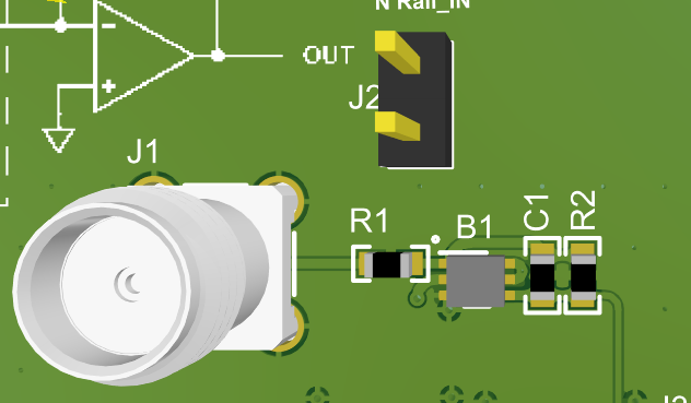
4-layer PCB

4-layer PCB

3D view:

3D view

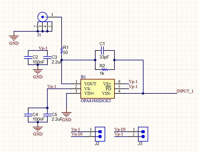
Schematic:

Schematic

So, the achieved SNR is 23.4 dB, but what should I get based on simulation is totally different 58 dB, would you please let me know why there is this much difference in the experimental and simulation results?

\$\endgroup\$
7
  • 1
    \$\begingroup\$ Take an FFT of your noise and see if there is something specific there. Show us details of your hardware - is it a PCB? Breadboard? What filtering and decoupling do you have on your board? \$\endgroup\$ Commented Jun 24 at 21:18
  • \$\begingroup\$ @Tom Carpenter thank you for your comment, I added the PCB and the schematic details in the post. \$\endgroup\$
    – Andromeda
    Commented Jun 24 at 21:25
  • 1
    \$\begingroup\$ How do you know the theoretical SNR? Is it just the SNR of amplifier, SNR of the whole electrical circuit alone, or SNR of random photons hitting the sensor, or is there a signal which gets some noise gets applied before photodiode sees it? (Assuming th sensor is a photodiode. You don't say what sensor it is). \$\endgroup\$
    – Justme
    Commented Jun 24 at 21:36
  • 2
    \$\begingroup\$ @Andromeda The transducer may pick up noie but even in pure rest state it is a noisy source, the tranmission line to amplifier is noisy, the amplifier itself is noisy, and even the feedback resistor generates thermal noise. Now depending on where the noise is generated, it gets added and/or amplified to the signal. \$\endgroup\$
    – Justme
    Commented Jun 24 at 21:56
  • 1
    \$\begingroup\$ 1) The PCB designations do not match with the circuit diagram. 2) The circuit diagram does not show R1 in series with the input. 3) There are no decoupling capacitors close to the power pins of the chip. 4) There is a PCB layout error on J2P1@Andromeda \$\endgroup\$
    – user319836
    Commented Jun 24 at 22:27

0

Your Answer

By clicking “Post Your Answer”, you agree to our terms of service and acknowledge you have read our privacy policy.