0
\$\begingroup\$

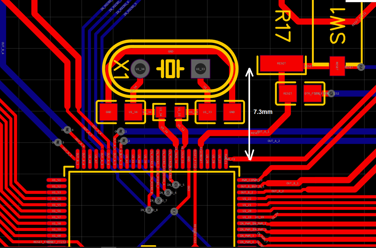
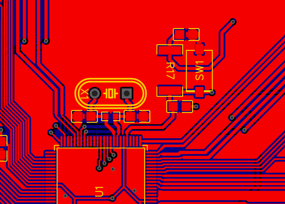
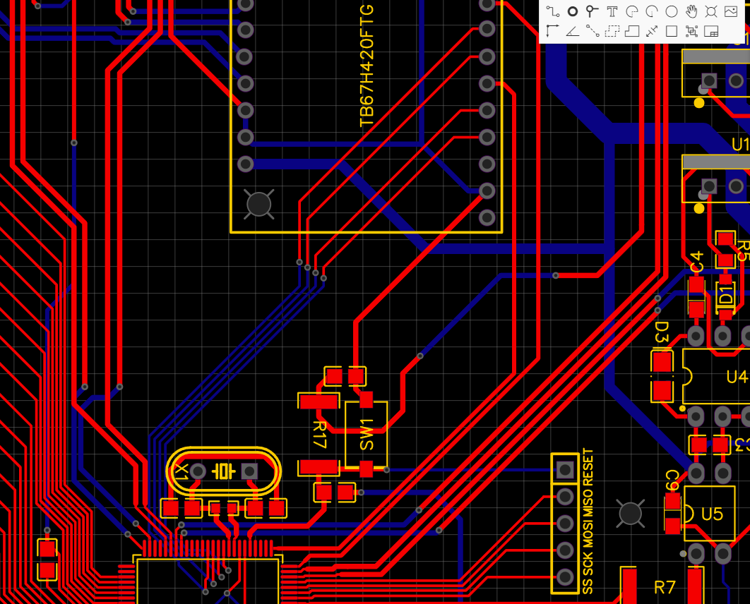
I thought I'd give an update to the changes I've made for my 2 layer PCB regarding the 16MHz crystal oscillator that I've added. Yes, this is a continuation of PCB layout for 16 MHz crystal oscillator. In short, I've corrected the schematic so the reset switch is grounded separately from the oscillator and I've moved them closed to their respective pins. I've marked the distance that I measured in Easyeda with white (~7.3mm). Is this layout acceptable now? I've opted to work with 2 layers only because I'm on a tight budget unfortunately and JLCPCB's 4 layer boards seem to cost more than double that of 2 layer.

enter image description here

enter image description here

enter image description here

Unfortunately, right next to the XTAL1 and XTAL2 pins are another set of 4 pins which I need to route to a motor driver. For this, I opted to use several via's beneath the microprocessor (IN_MICRO_5,6,7,8). I'm concerned that the trace length for these will be too long, even though they are only for setting the motor spin direction. The trace width for these lines is 0.25mm.

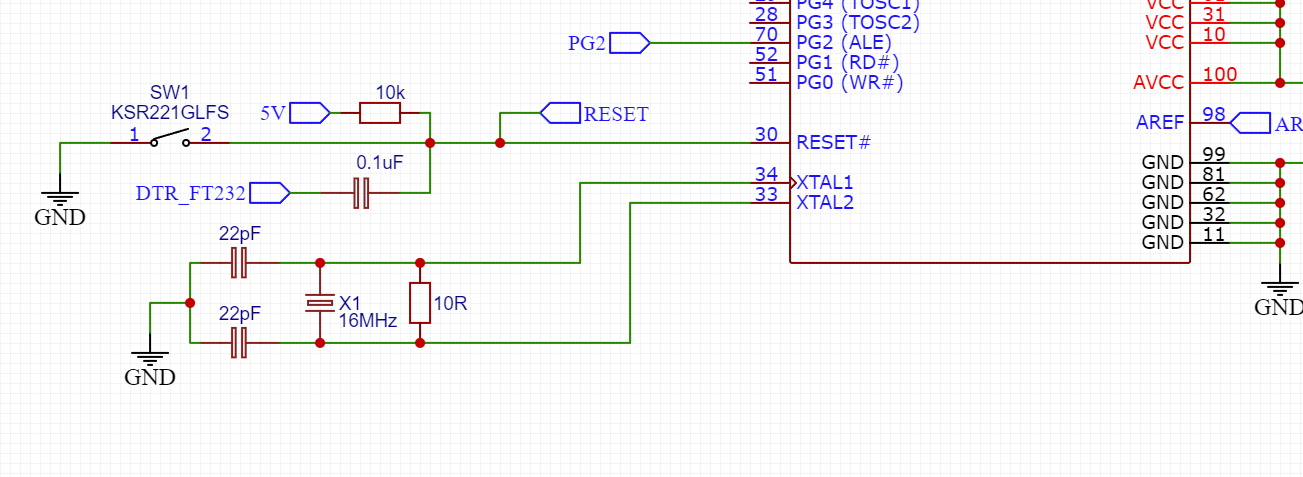
enter image description here

\$\endgroup\$
1
  • 1
    \$\begingroup\$ That cost increase will be more than offset by the time you waste debugging a 2 layer design IMHO \$\endgroup\$
    – Andy aka
    Commented Jul 3 at 9:30

1 Answer 1

1
\$\begingroup\$

The schematics are now correct regarding the crystal not being grounded from one leg.

But AVRs do not need a resistor between the crystal pins, and even if they did, the 10 ohms would be completely wrong value and the oscillator would fail to work. Generally these resistors, if needed, are in the 1 megaohm ballpark. You can remove the resistor or just leave it in the design but choose/set to not populate it during manufacture.

The crystal is now much closer to MCU and the wiring through crystal load caps to MCU pins look nice and short.

There are now a couple of things you may want to consider.

As crystal circuits are relatively sensitive, generally you don't wire other signals that toggle often near or under the crystal signals. You have somewhat good looking ground guard ring on the top but there is some wiring that crosses under the crystal wires, so it could be better, maybe on bottom layer there could be a ground fill so the crystal signals are only surrounded by ground on bottom and top layer.

Which brings up the next issue, as the ground surrounding the crystal and connects to caps appear to have no physical connection to MCU ground pin, so even if they do connect, it will be somewhere far away off the screen.

Ideally the crystal and caps should have a separate ground plane that only connects to MCU ground pin and conveniently the MCU XTAL pins have a GND right next to it.

Now, will it work as it is? Likely yes without issues, as long as you don't put the 10 ohm resistor between XTAL pins.

\$\endgroup\$
2
  • \$\begingroup\$ You are correct about the separate GND plane. Yet I think in this case even some stitching vias, next to the Caps could do wonders. \$\endgroup\$
    – S_G
    Commented Jul 3 at 11:08
  • \$\begingroup\$ @S_G The easiest way would be to just close the sub-millimeter gap between MCU GND pin right next to the crystal and the ground plane going from crystal to MCU. But yes, anyway, a few ground stitching vias should be added anyway (but the question was only about the crystal). \$\endgroup\$
    – Justme
    Commented Jul 3 at 11:14

Your Answer

By clicking “Post Your Answer”, you agree to our terms of service and acknowledge you have read our privacy policy.

Not the answer you're looking for? Browse other questions tagged or ask your own question.