2
\$\begingroup\$

With reference to similar issue: SPI device prevents ISP programming

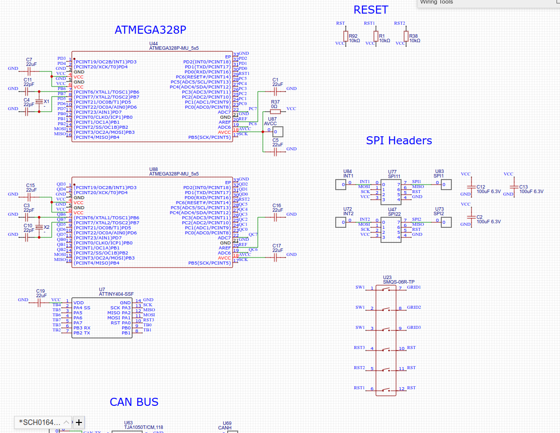
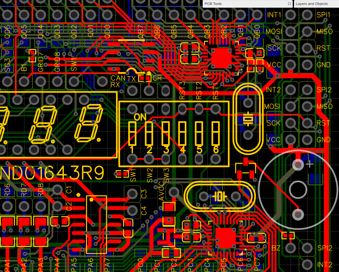
I have 2 ATMEGA328Ps with MOSI MISO and SCK permanently connected on the same board. At the time of printing the board my thoughts were to only connect the RST of the SPI to be programmed at a given time, therefore only reprogramming one chip via SPI header.

Turns out this was not a clever move. If both RST lines are connected to the programmer, both chips successfully reprogram simultaneously with the same identical sketch (not that useful having identical code on both chips).

But if either ATMEGA chip is disconnected from the programmers RST, neither chip will reprogram as the MOSI MISO and SCK from the other chip seem to interfere. I cannot fathom why.

Thinking along the lines of the opposite chip could be transimiting out of MISO interfering with the reprogramming, I flashed both chips (since I can do both at the same time) with a sketch that set MOSI, MISO and SCK as floating inputs and looped doing nothing else. but this did not seem to make any difference when then attempting to reprogram just one chip again.

I'm currently stumped on how to upload different sketches to the 2 integrated chips, as I cannot for the life of me see why the opposite chip could be interfering.

The top ATMEGA has 2 pull-up resistors to the right of it that are one for each ATMEGA reset holding each chip RST line high. 5 and 6 of the DIP-Switch between the two connect each RST1 and RST2 to the main RST (the idea being to toggle a switch during reprogramming disconnecting the RST from the chip that was NOT being re-programmed) but this fails as nether chip will program if eater 5 or 6 is toggled OFF.

Any suggestions on how I could try programming these chips with different code would be welcome. It's only really a learning curve but I would rather not abandon £80 of circuit boards without trying.

I also tried cutting the VCC track to the top ATMEGA with a Stanley knife (since that is exposed on the top side) but that failed as the chip still half powered off AVCC and still conflicted with programming the bottom ATMEGA.

enter image description here

enter image description here

This is a successful reprogram of both chips at the same time with the same sketch starting from RST falling low

enter image description here

enter image description here

enter image description here

This is a failed reprogram of the top chip (while the bottom chip RST is held high)

enter image description here

enter image description here

I have not really paid much attention to reprogramming ISP bits until now so in not sure if it helps.

EDIT: I am starting to feel like I am barking up the wrong tree, if I probe MOSI MISO and SCK. SCK is defiantly floating, I can inject 5v into it through a 3k resistor and it changes from high to low. yet MOSI and MISO both stay low, even when the RST to both ATMEGAs is held low. I think I need to check the MOSI MISO tracks some how before updating.

\$\endgroup\$
5
  • \$\begingroup\$ What is "eater chip"? \$\endgroup\$ Commented Jul 11 at 1:06
  • \$\begingroup\$ either ATMEGA328P, sorry, type, i am terrible at spelling \$\endgroup\$
    – Jay Dee
    Commented Jul 11 at 1:10
  • \$\begingroup\$ Why show layout instead of schematic? It's much harder to follow. If the programming pins are joined as said in the text, I'm not really sure what else there is to cover -- the linked question gives the reason. The solution is simple, "don't do that". Then, do you need a solution for your specific circuit and layout already fabricated? \$\endgroup\$ Commented Jul 11 at 1:14
  • \$\begingroup\$ yes, don't do that is a good answer, but i feel like there is (should be) some simple way to stop the conflict that im just not grasping, why MOSI MISO SCK are even conflicting in the first place if they are programmed floating input. sorry \$\endgroup\$
    – Jay Dee
    Commented Jul 11 at 1:23
  • \$\begingroup\$ @JayDee It depends on many thinga not shown in those not-very-easily-readable schematics. Are you sure about code setting them to floating inputs - because they should be floating inputs even if you don't touch the pins at all. Do they connect anywhere else or are they used for any other purpose? Trying to turn off one chip on the same bus by cutting power is the worst thing you can do to solve it, it seems you have not hears of IO pin protection diodes and how there should be no voltages present on unpowered chips or they try to power up via IO pins. \$\endgroup\$
    – Justme
    Commented Jul 11 at 4:55

2 Answers 2

0
\$\begingroup\$

There are a couple of things you can try:

  • If you are not using the SPI pin in the board for any other application, set them as inputs in your code. Flashed them both at the same time. Then the next time, you should be able to flash them independantly. The SPI pins of the second chip is simple input pins and should not interfere with the flashing.
  • If you are using the SPI pins as SPI or outputs, you can still achive this by adding a resistor between the SPI pins and the programming connector (for both chips). This should not cause any issue as long as the connections ore short or the load on the outputs are not draining much current. This way, even if a pin is set os output, the resistor will allow the signals on the programming port to program the other chip. I would start by adding 470R resitors.
\$\endgroup\$
1
  • \$\begingroup\$ i agree with you, but i feel like i have already tried and cannot understand why there is still a conflict even when pins are (to the best of my knowledge) floating. i have just added some ISP SPI logic \$\endgroup\$
    – Jay Dee
    Commented Jul 11 at 11:07
0
\$\begingroup\$

I have identified the cause of the problem, be it not ideal, at least it is logical.

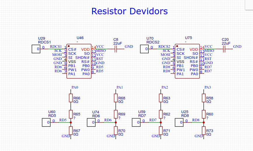
Elsewhere on the circuit is 2 Digital Potentiometers part number MCP42010T-I/SL that even when there RS pins are held to ground appear not to float MOSI and MISO.

Not very impressed with having to UN-solder / re-solder SOIC chips in order to re-program the board, but it does allow me to put code on the ATMEGAs that were otherwise useless.

Next time I will pay far more attention to breadboard testing chips before printing expensive boards.

enter image description here

\$\endgroup\$
2
  • \$\begingroup\$ You might take note of the description for SPI in this chip. SPI in general kind of works two ways: either as a straight-through shift register that some bits are tapped on/off of (this case), or as a single packet transaction (or incremental bytes thereof). The former can be chained like any shift register, and all devices updated at once; the latter is likely only point-to-point, or perhaps a terminal device. Since it's a write-only device, it seems unlikely you need MISO connected at all here. \$\endgroup\$ Commented Jul 11 at 14:36
  • \$\begingroup\$ thanks, I will try it on one to see, I can scrape the MISO pad off the board before punting a chip back to see what happens, the boards are useful for somthing even if a pot does not work, they were quite useless without a processor. \$\endgroup\$
    – Jay Dee
    Commented Jul 11 at 15:51

Your Answer

By clicking “Post Your Answer”, you agree to our terms of service and acknowledge you have read our privacy policy.

Not the answer you're looking for? Browse other questions tagged or ask your own question.