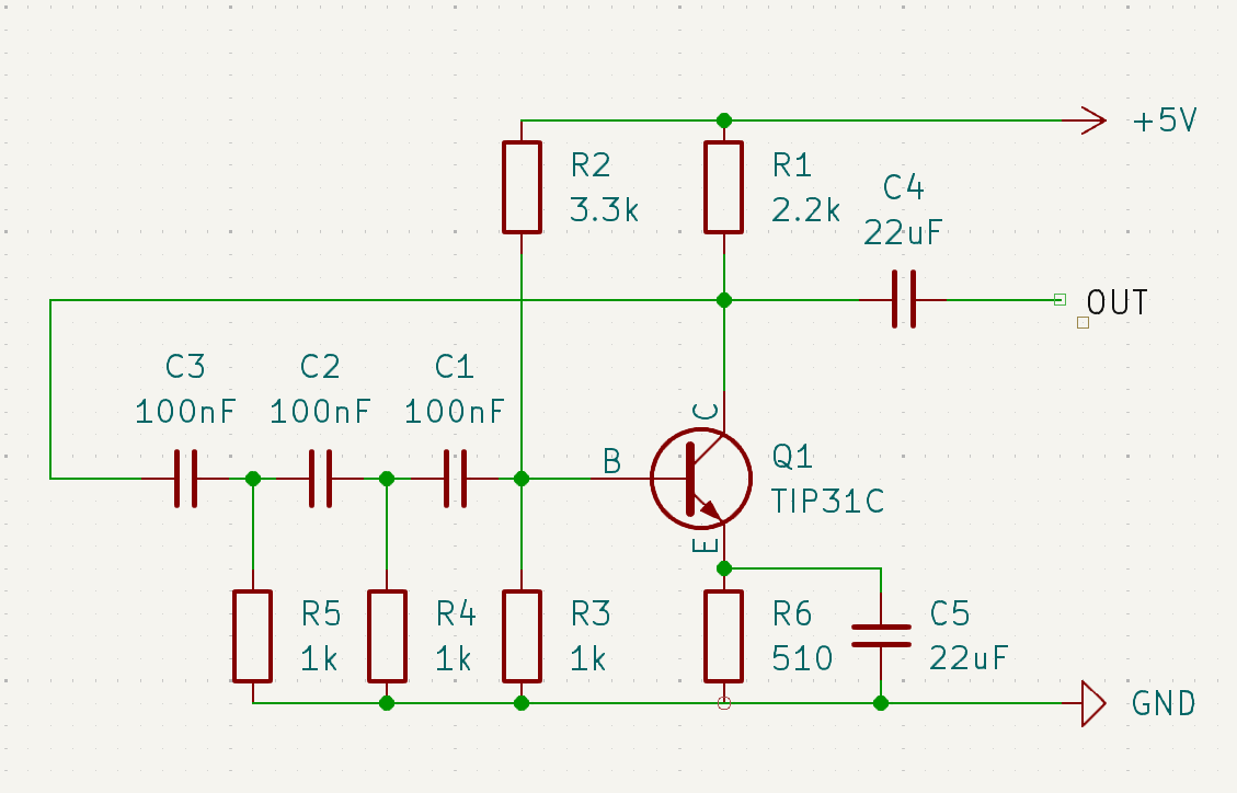
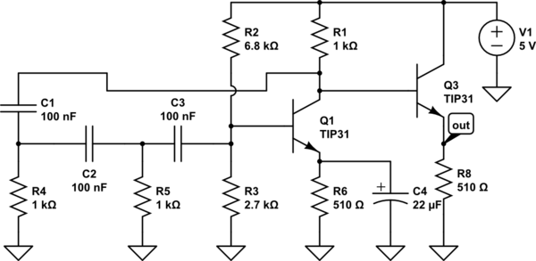
first thoughts
The RC phase shift oscillator is often studied in a somewhat more ideal circumstance; usually using an opamp to make things a bit more idealized. Using a single bipolar transistor as the amplifier is significantly less ideal. So it must be incorporated into the prediction and/or design of output frequency.
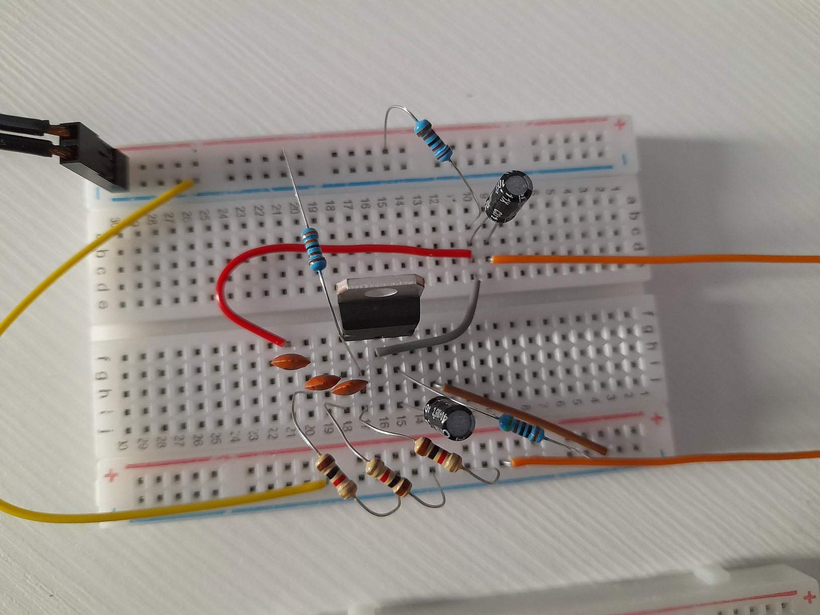
You are using a solderless breadboard. These have significant capacitance between adjacent rows, for example: significant in the sense of capacitances that are part of the bipolar transistor, anyway. To reduce the risk of difficulties, the three phase-shift capacitor values should have magnitudes larger than \$1\:\text{nF}\$. And more would be better. I'd probably go further and avoid using capacitors with values less than \$2.2\:\text{nF}\$.
passive RC phase-shift section
A surface glance at the circuit tells me that there is a source impedance (the collector resistor's value, modified slightly by the Early Effect) that drives the passive RC phase-shift section. And there's also a load impedance, which takes into account your circuit's \$R_3\$ value and modifies it -- substantially -- because of the way you have the emitter bypassed with a capacitor.
The result is something that looks about like this:

simulate this circuit – Schematic created using CircuitLab
The value of \$R_{_\text{LOAD}}\$ (which is really a \$Z_{_\text{LOAD}}\$ due to the bypass cap) takes into account many details of the bipolar transistor section, including your value of \$R_3\$ and the small-signal value of \$r_\pi\$, among other things. The way you have the stage arranged, with the capacitor completely bypassing the emitter resistor, the value of \$r_\pi\$ will likely dominate. For that reason alone, I'd alter your circuit slightly. I'll get to that soon.
The value of \$R_{_\text{SOURCE}}\$ takes into account your value of \$R_1\$ and also the small-signal value of the Early Effect, \$r_o\$. Here \$R_1\$ will dominate.
Using my nomenclature for the phase-shift section illustrated above and setting\$R_1=R_2=R\$ and \$C_1=C_2=C_3=C\$, then the frequency selected is likely to be close to:
$$f_0=\frac1{2\pi\,C\,\sqrt{R_{_\text{LOAD}}\,\cdot \,R_{_\text{SOURCE}}+3R\cdot\left(R+R_{_\text{LOAD}}+R_{_\text{SOURCE}}\right)}}$$
(I won't go into the details of how I got that. But it's just finding the transfer function. Here, it's numerator is an odd power of s, so I set the real part of the denominator equal to zero and solved. An even power in the numerator, had that been the case, would have meant setting the imaginary part of the denominator to zero before solving.)
modifying your design
I'd avoid completely bypassing the emitter resistor and add another emitter resistor. But other than that I'd keep your structure. The reason is that different transistors may behave slightly differently and it may be helpful to be able to insert a small-valued resistor in series with the bypass capacitor. I think it may help you when switching transistors around.
I would definitely avoid power bipolars for a circuit like this. So I would not use a TIP31. Power bipolars have a variety of parasitics, including leakage currents, that intrude and make this kind of circuit harder to design and get working right. I know it is what you have. But you should get some small signal bipolars for this circuit. Later, when you feel up to the challenges, you can work on using the TIP31. It's enough of a problem that I'm certainly going to avoid discussing the TIP31 here.
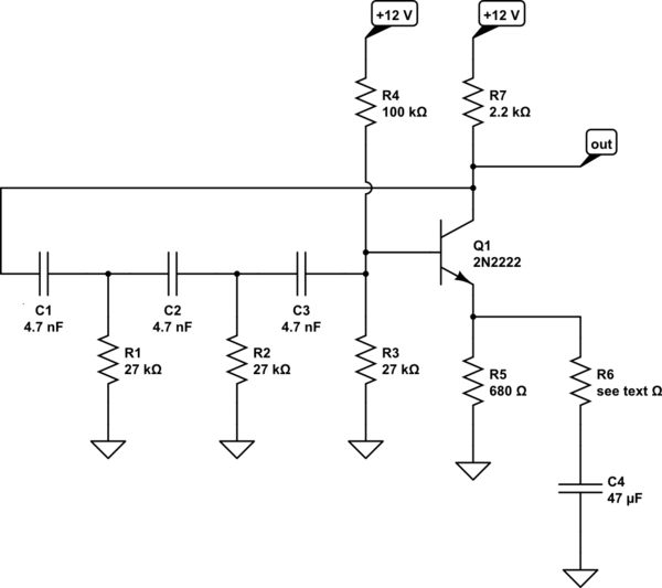
Here is the schematic with an altered emitter bypass arrangement and using my own part numbering, plus a small signal bipolar:

simulate this circuit
I also changed the power supply rail to \$+12\:\text{V}\$. I hope you don't mind.
Lower power supply rails complicate some of what I have to say as I need to consider more details and therefore write more to convey them. Besides, I'd recommend that you start with a larger power supply rail, anyway, and get that working right before considering low-voltage supply rails. There's just more to worry over as you lower the voltage used to supply the circuit and it will simplify your life a little to use larger supply voltages when starting out.
Let's start with your collector resistor value -- I like it. I'd set the quiescent collector voltage to about half the supply rail, so this means that the quiescent collector current will be \$\frac{6\:\text{V}}{2.2\:\text{k}\Omega}\approx 2.7 \:\text{mA}\$. That's in a normal range for small signal BJTs, which I'm recommending.
That's a start.
Now \$r_e^{\:'}\approx 10\:\Omega\$. Assuming we don't care about thermal issues for now, we can tentatively set \$R_6=0\:\Omega\$ and work out that with \$100\le \beta\le 300\$ that \$1\:\text{k}\Omega \le r_\pi\le 3\:\text{k}\Omega\$. If that is to dominate the circuit loading, then \$R_3\$ must be about \$10\times\$ that.
This is also about \$10\times\$ the value of collector resistor \$R_7\$, which sits well with me. But to really make \$r_\pi\$ dominate, I'll set \$R_3=27\:\text{k}\Omega\$. It would be attractive if \$R_1=R_2=R_3\$. So I'll do that, too.
Given the quiescent collector current, I know I'd like a DC bias current of something near or above \$100\:\mu\text{A}\$ through \$R_3\$. That would suggest about \$2.7\:\text{V}\$ at the base and about \$2\:\text{V}\$ at the emitter. A bit high, but certainly acceptable. If so, then this means about \$93\:\text{k}\Omega\$ for \$R_4\$. I'll just go and make \$R_4=100\:\text{k}\Omega\$. That makes the base voltage closer to \$2.5\:\text{V}\$.
The emitter voltage is now about \$1.8\:\text{V}\$ (in my head), so this suggests \$R_5\approx 680\:\Omega\$. And that's what I'll use.
Now we have the frequency issue to deal with. Which is just a matter of setting up the value for the capacitors. The above formula re-arranges as:
$$C=\frac1{2\pi\,f_0\,\sqrt{R_{_\text{LOAD}}\,\cdot \,R_{_\text{SOURCE}}+3R\cdot\left(R+R_{_\text{LOAD}}+R_{_\text{SOURCE}}\right)}}$$
I estimate that \$R_{_\text{SOURCE}}\approx 2.1\:\text{k}\Omega\$ (\$R_7\$ and adding in the Early Effect) and that \$R_{_\text{LOAD}}\approx r_\pi\$ (because I made sure \$r_\pi\$ dominates the phase-shift section's loading), which will be somewhere in the range indicated earlier.
So from the above equation I then find that \$C\approx 4.7\:\text{nF}\$. So that's the value.
Start out as you already have, with \$R_6=0\:\Omega\$. But play around with it up to the maximum value I mentioned before.
simulation
I very recently downloaded QSPICE and have started to play with it. I decided to see what it does with the above schematic. (I'll use a non-zero \$R_6=2.2\:\Omega\$.)
First off, I need calculate the frequency using SageMath/SymPy. The bipolar model I'll use will have \$\beta\approx 200\$, so I'll assume \$R_{_\text{LOAD}}\approx 2\:\text{k}\Omega\$.
(1/(2*pi*C*sqrt(Rload*Rsource+3*R*(R+Rload+Rsource)))).subs({R:27e3,C:4.7e-9,Rsource:2.1e3,Rload:2000}).n()
674.120958877630
So the prediction is \$f_0\approx 674 \:\text{Hz}\$.

I'm actually a little surprised it is that close. And since I didn't include \$R_6=2.2\:\Omega\$ in my estimate for the load, let's see what that does when it is included:
(1/(2*pi*C*sqrt(Rload*Rsource+3*R*(R+Rload+Rsource)))).subs({R:27e3,C:4.7e-9,Rsource:2.1e3,Rload:200*(10+2.2)}).n()
669.289215790583
Okay, keeping in mind that I'm only using an approximate value for \$r_\pi\$, I have to say that the formula does appear to get close to the mark that QSPICE suggests. Good to see.
notes
With \$C_4=47\:\mu\text{F}\$ and \$f_0\approx 650\:\text{Hz}\$ the impedance is about \$5\:\Omega\$. (In quadrature.) If significantly lower frequencies are sought, then \$C_4\$ should be made proportionately larger.
Also, for \$R\approx 10\cdot R_{_\text{LOAD}}\$ and \$R\approx 10\cdot R_{_\text{SOURCE}}\$, which is close to the above case, then set \$\gamma=1.9\$. And for \$R\gg R_{_\text{LOAD}}\$ and \$R\gg R_{_\text{SOURCE}}\$ set \$\gamma=\sqrt{3}\$.
Then it appears there's a fairly simple equation: \$f_0\approx\frac1{2\pi\,\gamma\,R\,C}\$.

