0
\$\begingroup\$

I am looking at different CPU micro-architectures.

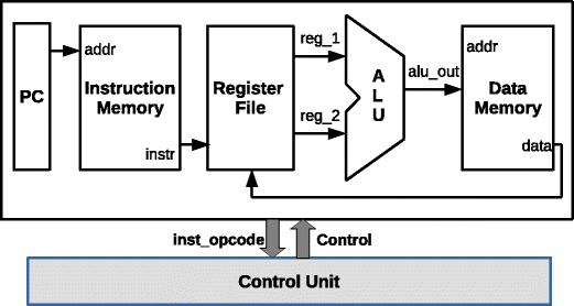
Frequently, it happens that the ROM is supposed to contain only instruction data. See below for an example:

enter image description here

In such design, how is the CPU supposed to access constant data stored in ROM ? It seems that it is just impossible. If this is correct, then how is the compiler/linker supposed to know it so it will not try to put data in the ROM ? And how are constant data handled in this case ?

EDIT: I reworded my question below because it was not totally explicit.

Let's suppose that we have a constant data or a literal stored in ROM, but too large to fit in an instruction.

To access that data, the compiler will generate a load instruction containing its address.

How will the CPU handle/execute this instruction ? It will require to do two reads from the ROM at the same time: one for the data, and one to fetch the next instruction.

Does the ROM contain two read ports ?

\$\endgroup\$
5
  • 2
    \$\begingroup\$ It's fairly common on embedded systems that you have multiple types of memory (ROM, DRAM, SRAM, etc) that have different restrictions. When you setup your tool chain (or more likely download one setup by the vendor), the linker will be configured as needed to put code/data/etc where they belong. Often times there will be different preprocessor defines as well that let the programmer specify which memory to allocate into. \$\endgroup\$ Commented Jul 29 at 13:51
  • \$\begingroup\$ @user1850479 in such a system, if the user decides to tell the linker to put some constant data in ROM, how do the CPU process a load instruction pointing to this data ? Does the ROM have dual port, so the CPU can read the data and fetch the next instruction at the same time ? \$\endgroup\$
    – wbs2422
    Commented Jul 29 at 21:05
  • \$\begingroup\$ You'd have to check the datasheet for the specific device to see what the access restrictions are and how these things are handled. \$\endgroup\$ Commented Jul 29 at 23:18
  • \$\begingroup\$ @user1850479 actually I am trying to design a CPU for learning purpose, and I'm wondering how to handle the memory management module \$\endgroup\$
    – wbs2422
    Commented Aug 1 at 7:30
  • \$\begingroup\$ Often there is also an instruction that loads data from instruction ROM. This takes two cycles, of course, since the instruction ROM can't load an instruction at the same time. \$\endgroup\$ Commented Sep 23 at 21:21

3 Answers 3

2
\$\begingroup\$

Most CPU architectures include a way to store data in the instruction stream, such as "move immediate" on register machines, or "literal" on stack machines. If the machine has a Harvard architecture, with separate code and data spaces, sequences of such instructions can be used to initialize data memory.

\$\endgroup\$
10
  • \$\begingroup\$ Let's suppose that we want to access a data stored in ROM but too large to fit in an instruction, for example a character string. The compiler will generate a load instruction containing the address of the data. How is the CPU processing such instruction ? Because at the same time it must do two reads from the ROM : one for the data, and one for fetching the next instruction. Does the ROM have two ports ? \$\endgroup\$
    – wbs2422
    Commented Jul 29 at 21:13
  • 1
    \$\begingroup\$ Your question has a diagram of a Harvard architecture machine. Such a machine would have two separate ROMs, one for instructions and one for data. So yes, both accesses could occur in parallel. On a von Neumann machine, the accesses would occur sequentially, so a single ROM could contain both instructions and data. \$\endgroup\$
    – Dave Tweed
    Commented Jul 29 at 21:24
  • \$\begingroup\$ Oh, I see ! So "data memory" does not necessarily correspond to a RAM, but could be a mix of a ROM and a RAM ? And in a von Neumann machine, the next instruction would be fetched one cycle after the reading of the data ? \$\endgroup\$
    – wbs2422
    Commented Jul 29 at 21:29
  • 1
    \$\begingroup\$ Yes. The alternative would be to have a start-up function that initializes data in RAM before the main program starts. \$\endgroup\$
    – Dave Tweed
    Commented Jul 29 at 21:31
  • 2
    \$\begingroup\$ A linker for a Harvard architecture machine would already be aware that there are two separate address spaces, and manage them separately. The naming of sections and their mapping into the address spaces would depend on the conventions used on a specific machine. We're talking generalities here. \$\endgroup\$
    – Dave Tweed
    Commented Jul 29 at 22:02
1
\$\begingroup\$

In a Von Neumann architecture, ROM would be memory-mapped and thus accessed by the same move instructions as RAM and support the same address modes. Move immediates also may be used to get ROM values.

In a Harvard architecture, the code and data spaces are separated. However, move immediates can still be used for loading ROM constants, as the immediate values are part of the instruction and fetched with it.

More general access to ROM-based constants use a 'bypass' path for values fetched from ROM and stored in registers. An example is the 8051 MOVC, a special instruction which accesses ROM as if it were memory-mapped and loads the value to the accumulator.

\$\endgroup\$
1
  • \$\begingroup\$ I see, I'll have a look at the 8051 architecture, and try to get some ideas from it, thanks ! (sorry for late answer) \$\endgroup\$
    – wbs2422
    Commented Aug 1 at 7:36
0
\$\begingroup\$

The TI TM4C129 series ARM Cortex-M4F based microcontrollers have the option of Execute-Only Protection for the flash. Section 8.2.3.5 Execute-Only Protection of the datasheet contains the following, which recognises the impact on the program:

Execute-only protection prevents both modification and visibility to a protected flash block. ...

Literal data introduces a complication to the protection mechanism. When C code is compiled and linked, literal data (constants, and so on) is typically placed in the text section, between functions, by the compiler. The literal data is accessed at run time through the use of the LDR instruction, which loads the data from memory using a PC-relative memory address. The execution of the LDR instruction generates a read transaction across the Cortex-M3's DCode bus, which is subject to the execute-only protection mechanism. If the accessed block is marked as execute only, the transaction is blocked, and the processor is prevented from loading the constant data and, therefore, inhibiting correct execution.

The TI ARM Optimizing C/C++ Compiler v20.2.0.LTS has the following option in 2.3.4 Run-Time Model Options which allows the compiler to know not to place constants in the "execute code only" section:

--embedded_constants={on|off} By default the compiler embeds constants in functions. These constants can include literals, addresses, strings, etc. This is a problem if you wants to prevent reads from a memory region that contains only executable code. To enable the generation of "execute only code", the compiler provides the --embedded_constants=[on|off] option. If the option is not specified, it is assumed to be on. The option is available on the following devices: Cortex-A8, Cortex-M3, Cortex-M4, and Cortex-R4.

While the question is asking a general architecture question, the above example demonstrates how the compilers for microcontrollers may address the problem.


In response to the comment:

So, if my understanding is correct, the linker will put the literal in a dedicated flash memory area. Then how do the CPU access this data while also fetching the next instruction ? It will require to do two reads of the same flash memory module at the same time – Wheatley

For the example of the ARM Cortex-M4 there are two buses in the Code memory map:

  • Instruction fetches are performed over the ICode bus.
  • Data accesses are performed over the DCode bus.

The answer in STM32 I-CODE and D-CODE buses shows a Flash interface which arbitrates access from the ICode and DCode buses to the flash memory. While there is a single flash memory, it has a wider data interface (128 bits) than the ICode and DCode buses (32-bit data bus). Prefetching or caching in flash memory module may hide some latency as a result of accesses from both the ICode and DCode buses.

\$\endgroup\$
3
  • \$\begingroup\$ So, if my understanding is correct, the linker will put the literal in a dedicated flash memory area. Then how do the CPU access this data while also fetching the next instruction ? It will require to do two reads of the same flash memory module at the same time \$\endgroup\$
    – wbs2422
    Commented Jul 29 at 21:19
  • \$\begingroup\$ @Wheatley I have tried to update the answer in response to your comment. \$\endgroup\$ Commented Jul 29 at 22:14
  • \$\begingroup\$ (sorry for late answer) : regarding the link, what does it mean "I-CODE and D-CODE busses cannot access the flash memory independently, they do however access the flash interface independently" ? If my understanding of the schematic is correct, the CPU is "stalled" when accessing the flash through the data bus, meaning that the program counter is not updated during this cycle ? \$\endgroup\$
    – wbs2422
    Commented Aug 1 at 7:46

Your Answer

By clicking “Post Your Answer”, you agree to our terms of service and acknowledge you have read our privacy policy.

Not the answer you're looking for? Browse other questions tagged or ask your own question.